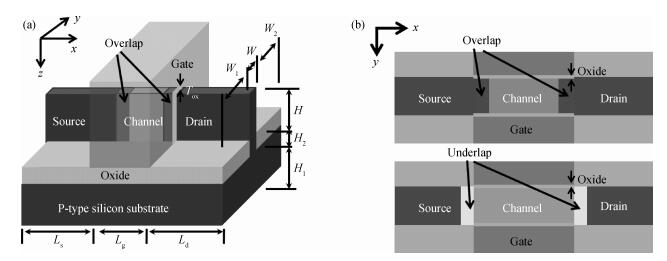
Fig. 1.
Schematic view of bulk FinFET. (a) 3D view. (b) x-y plane view
SEMICONDUCTOR DEVICES
Juncheng Wang1, Gang Du1, , Kangliang Wei1, Lang Zeng1, Xing Zhang1 and Xiaoyan Liu1
Corresponding author: Du Gang, Email:gangdu@pku.edu.cn
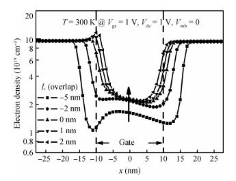
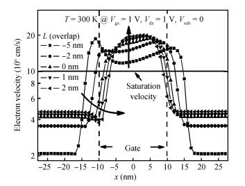
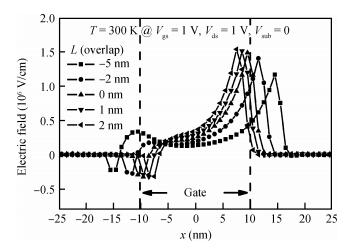
Abstract: We investigate the influence of gate-source/drain (G-S/D) misalignment on the performance of bulk fin field effect transistors (FinFETs) through the three-dimensional (3D) full band Monte Carlo simulator. Several scattering mechanisms, such as acoustic and optical phonon scattering, ionized impurity scattering, impact ionization scattering and surface roughness scattering are considered in our simulator. The influence of G-S/D overlap and underlap on the on-states performance and carrier transport of bulk FinFETs are mainly discussed in our work. Our results show that the on-states currents increase with the increment of G-D/S overlap length and the positions of a potential barrier and average electron energy maximum vary with the G-D/S overlap length. The carrier transport phenomena in bulk FinFETs are due to the effect of scattering and the electric field in the overlap/underlap regime.
Keywords: bulk FinFET, gate-source/drain misalignment, 3D Monte Carlo simulation, carrier transport
| [1] |
Hisamoto D, Lee W C, Kedzierski J, et al. FinFET——a self-aligned double-gate MOSFET scalable to 20 nm. IEEE Trans Electron Devices, 2000, 47(12):2320 doi: 10.1109/16.887014
|
| [2] |
Choi Y K, Lindert N, Xuan P, et al. Sub-20 nm CMOS FinFET technologies. International Electron Devices Meeting Technical Digest, 2001:421 http://ieeexplore.ieee.org/document/979526/
|
| [3] |
Landgraf E, Rosner W, Stadele M, et al. Influence of crystal orientation and body doping on trigate transistor performance. Solid-State Electron, 2006, 50:38 doi: 10.1016/j.sse.2005.10.041
|
| [4] |
Bin Y, Leland C, Ahmed S, et al. FinFET scaling to 10 nm gate length. International Electron Devices Meeting Technical Digest, 2002:251 http://ieeexplore.ieee.org/document/1175825/authors
|
| [5] |
Hu C. New sub-20 nm transistors——why and how. Design Automation Conference (DAC), 2011:460
|
| [6] | |
| [7] |
Park T, Choi S, Lee D H, et al. Fabrication of bodytied FinFETs (omega MOSFETs) using bulk Si wafers. VLSI Symp Tech Dig, 2003:135
|
| [8] |
Okano K, Izumida T, Kawasaki H, et al. Process integration technology and device characteristics of CMOS FinFET on bulk silicon substrate with sub-10 nm fin width and 20 nm gate length. International Electron Devices Meeting Technical Digest, 2005:721 http://ieeexplore.ieee.org/document/1609454/authors
|
| [9] |
Manoj C R, Meenakshi N, Dhanya V, et al. Device optimization of bulk FinFETs and its comparison with SOI FinFETs. International Workshop on Physics of Semiconductor Devices (IWPSD), 2007:134
|
| [10] |
Sun X, Moroz V, Damrongplasit N, et al. Variation study of the planar ground-plane bulk MOSFET, SOI FinFET, and trigate bulk MOSFET designs. IEEE Trans Electron Devices, 2011, 58(10):3294 doi: 10.1109/TED.2011.2161479
|
| [11] |
Trivedi V, Fossum J G, Chowdhury M M. Nanoscale FinFETs with gate-source/drain underlap. IEEE Trans Electron Devices, 2005, 52(1):56 doi: 10.1109/TED.2004.841333
|
| [12] |
Yang J W, Harris H R, Hussain M M, et al. Enhanced performance and SRAM stability in FinFET with reduced process steps for source/drain doping. VLSI Technology, Systems and Applications (VLSI-TSA), 2008:20
|
| [13] |
Kim S H, Fossum J G. Design optimization and performance projections of double-gate FinFETs with gate-source/drain underlap for SRAM application. IEEE Trans Electron Devices, 2007, 54(8):1934 doi: 10.1109/TED.2007.901070
|
| [14] |
Zhang W, Du G, Li Q, et al. A 3D parallel Monte Carlo simulator for semiconductor devices. International Workshop on Computational Electronics (IWCE), 2009:1 http://ieeexplore.ieee.org/document/5091078/authors
|
| [15] |
Du G, Zhang W, Wang J, et al. Study of 20 nm bulk FINFET by using 3D full band Monte Carlo method with effective potential quantum correction. IEEE International Conference on Solid-State and Integrated Circuit Technology (ICSICT), 2010:1952
|
| [16] |
Du G, Liu X Y, Xia Z L, et al. Simulation of Si and Ge UTB MOSFETs using Monte Carlo method based on the quantum Boltzmann equation. International Workshop on Computational Electronics (IWCE), 2004:186
|
| [17] |
Du G, Liu X Y, Xia Z L, et al. Monte Carlo simulation of p-and n-channel GOI MOSFETs by solving the quantum Boltzmann equation. IEEE Trans Electron Devices, 2005, 52(10):2258 doi: 10.1109/TED.2005.856806
|
| [18] |
Wei K L, Liu X Y, Du G, et al. Simulation of carrier transport in heterostructures using the 2D self-consistent full-band ensemble Monte Carlo method. Journal of Semiconductors, 2010, 31(8):1364 http://www.jos.ac.cn/bdtxben/ch/reader/view_abstract.aspx?file_no=10011601&flag=1
|
| [19] |
Pham A T, Nguyen C D, Jungemann C, et al. A semiempirical surface scattering model for quantum corrected Monte Carlo simulation of strained Si-nMOSFETs. European Solid-State Device Research Conference (ESSDERC), 2005:293
|
Table 1. Default parameters used in this work

|
| [1] |
Hisamoto D, Lee W C, Kedzierski J, et al. FinFET——a self-aligned double-gate MOSFET scalable to 20 nm. IEEE Trans Electron Devices, 2000, 47(12):2320 doi: 10.1109/16.887014
|
| [2] |
Choi Y K, Lindert N, Xuan P, et al. Sub-20 nm CMOS FinFET technologies. International Electron Devices Meeting Technical Digest, 2001:421 http://ieeexplore.ieee.org/document/979526/
|
| [3] |
Landgraf E, Rosner W, Stadele M, et al. Influence of crystal orientation and body doping on trigate transistor performance. Solid-State Electron, 2006, 50:38 doi: 10.1016/j.sse.2005.10.041
|
| [4] |
Bin Y, Leland C, Ahmed S, et al. FinFET scaling to 10 nm gate length. International Electron Devices Meeting Technical Digest, 2002:251 http://ieeexplore.ieee.org/document/1175825/authors
|
| [5] |
Hu C. New sub-20 nm transistors——why and how. Design Automation Conference (DAC), 2011:460
|
| [6] | |
| [7] |
Park T, Choi S, Lee D H, et al. Fabrication of bodytied FinFETs (omega MOSFETs) using bulk Si wafers. VLSI Symp Tech Dig, 2003:135
|
| [8] |
Okano K, Izumida T, Kawasaki H, et al. Process integration technology and device characteristics of CMOS FinFET on bulk silicon substrate with sub-10 nm fin width and 20 nm gate length. International Electron Devices Meeting Technical Digest, 2005:721 http://ieeexplore.ieee.org/document/1609454/authors
|
| [9] |
Manoj C R, Meenakshi N, Dhanya V, et al. Device optimization of bulk FinFETs and its comparison with SOI FinFETs. International Workshop on Physics of Semiconductor Devices (IWPSD), 2007:134
|
| [10] |
Sun X, Moroz V, Damrongplasit N, et al. Variation study of the planar ground-plane bulk MOSFET, SOI FinFET, and trigate bulk MOSFET designs. IEEE Trans Electron Devices, 2011, 58(10):3294 doi: 10.1109/TED.2011.2161479
|
| [11] |
Trivedi V, Fossum J G, Chowdhury M M. Nanoscale FinFETs with gate-source/drain underlap. IEEE Trans Electron Devices, 2005, 52(1):56 doi: 10.1109/TED.2004.841333
|
| [12] |
Yang J W, Harris H R, Hussain M M, et al. Enhanced performance and SRAM stability in FinFET with reduced process steps for source/drain doping. VLSI Technology, Systems and Applications (VLSI-TSA), 2008:20
|
| [13] |
Kim S H, Fossum J G. Design optimization and performance projections of double-gate FinFETs with gate-source/drain underlap for SRAM application. IEEE Trans Electron Devices, 2007, 54(8):1934 doi: 10.1109/TED.2007.901070
|
| [14] |
Zhang W, Du G, Li Q, et al. A 3D parallel Monte Carlo simulator for semiconductor devices. International Workshop on Computational Electronics (IWCE), 2009:1 http://ieeexplore.ieee.org/document/5091078/authors
|
| [15] |
Du G, Zhang W, Wang J, et al. Study of 20 nm bulk FINFET by using 3D full band Monte Carlo method with effective potential quantum correction. IEEE International Conference on Solid-State and Integrated Circuit Technology (ICSICT), 2010:1952
|
| [16] |
Du G, Liu X Y, Xia Z L, et al. Simulation of Si and Ge UTB MOSFETs using Monte Carlo method based on the quantum Boltzmann equation. International Workshop on Computational Electronics (IWCE), 2004:186
|
| [17] |
Du G, Liu X Y, Xia Z L, et al. Monte Carlo simulation of p-and n-channel GOI MOSFETs by solving the quantum Boltzmann equation. IEEE Trans Electron Devices, 2005, 52(10):2258 doi: 10.1109/TED.2005.856806
|
| [18] |
Wei K L, Liu X Y, Du G, et al. Simulation of carrier transport in heterostructures using the 2D self-consistent full-band ensemble Monte Carlo method. Journal of Semiconductors, 2010, 31(8):1364 http://www.jos.ac.cn/bdtxben/ch/reader/view_abstract.aspx?file_no=10011601&flag=1
|
| [19] |
Pham A T, Nguyen C D, Jungemann C, et al. A semiempirical surface scattering model for quantum corrected Monte Carlo simulation of strained Si-nMOSFETs. European Solid-State Device Research Conference (ESSDERC), 2005:293
|


Article views: 2826 Times PDF downloads: 48 Times Cited by: 0 Times
Received: 21 August 2012 Revised: 17 September 2012 Online: Published: 01 April 2013
| Citation: |
Juncheng Wang, Gang Du, Kangliang Wei, Lang Zeng, Xing Zhang, Xiaoyan Liu. Influence of gate-source/drain misalignment on the performance of bulk FinFETs by a 3D full band Monte Carlo simulation[J]. Journal of Semiconductors, 2013, 34(4): 044005. doi: 10.1088/1674-4926/34/4/044005
****
J C Wang, G Du, K L Wei, L Zeng, X Zhang, X Y Liu. Influence of gate-source/drain misalignment on the performance of bulk FinFETs by a 3D full band Monte Carlo simulation[J]. J. Semicond., 2013, 34(4): 044005. doi: 10.1088/1674-4926/34/4/044005.

|
| [1] |
Hisamoto D, Lee W C, Kedzierski J, et al. FinFET——a self-aligned double-gate MOSFET scalable to 20 nm. IEEE Trans Electron Devices, 2000, 47(12):2320 doi: 10.1109/16.887014
|
| [2] |
Choi Y K, Lindert N, Xuan P, et al. Sub-20 nm CMOS FinFET technologies. International Electron Devices Meeting Technical Digest, 2001:421 http://ieeexplore.ieee.org/document/979526/
|
| [3] |
Landgraf E, Rosner W, Stadele M, et al. Influence of crystal orientation and body doping on trigate transistor performance. Solid-State Electron, 2006, 50:38 doi: 10.1016/j.sse.2005.10.041
|
| [4] |
Bin Y, Leland C, Ahmed S, et al. FinFET scaling to 10 nm gate length. International Electron Devices Meeting Technical Digest, 2002:251 http://ieeexplore.ieee.org/document/1175825/authors
|
| [5] |
Hu C. New sub-20 nm transistors——why and how. Design Automation Conference (DAC), 2011:460
|
| [6] | |
| [7] |
Park T, Choi S, Lee D H, et al. Fabrication of bodytied FinFETs (omega MOSFETs) using bulk Si wafers. VLSI Symp Tech Dig, 2003:135
|
| [8] |
Okano K, Izumida T, Kawasaki H, et al. Process integration technology and device characteristics of CMOS FinFET on bulk silicon substrate with sub-10 nm fin width and 20 nm gate length. International Electron Devices Meeting Technical Digest, 2005:721 http://ieeexplore.ieee.org/document/1609454/authors
|
| [9] |
Manoj C R, Meenakshi N, Dhanya V, et al. Device optimization of bulk FinFETs and its comparison with SOI FinFETs. International Workshop on Physics of Semiconductor Devices (IWPSD), 2007:134
|
| [10] |
Sun X, Moroz V, Damrongplasit N, et al. Variation study of the planar ground-plane bulk MOSFET, SOI FinFET, and trigate bulk MOSFET designs. IEEE Trans Electron Devices, 2011, 58(10):3294 doi: 10.1109/TED.2011.2161479
|
| [11] |
Trivedi V, Fossum J G, Chowdhury M M. Nanoscale FinFETs with gate-source/drain underlap. IEEE Trans Electron Devices, 2005, 52(1):56 doi: 10.1109/TED.2004.841333
|
| [12] |
Yang J W, Harris H R, Hussain M M, et al. Enhanced performance and SRAM stability in FinFET with reduced process steps for source/drain doping. VLSI Technology, Systems and Applications (VLSI-TSA), 2008:20
|
| [13] |
Kim S H, Fossum J G. Design optimization and performance projections of double-gate FinFETs with gate-source/drain underlap for SRAM application. IEEE Trans Electron Devices, 2007, 54(8):1934 doi: 10.1109/TED.2007.901070
|
| [14] |
Zhang W, Du G, Li Q, et al. A 3D parallel Monte Carlo simulator for semiconductor devices. International Workshop on Computational Electronics (IWCE), 2009:1 http://ieeexplore.ieee.org/document/5091078/authors
|
| [15] |
Du G, Zhang W, Wang J, et al. Study of 20 nm bulk FINFET by using 3D full band Monte Carlo method with effective potential quantum correction. IEEE International Conference on Solid-State and Integrated Circuit Technology (ICSICT), 2010:1952
|
| [16] |
Du G, Liu X Y, Xia Z L, et al. Simulation of Si and Ge UTB MOSFETs using Monte Carlo method based on the quantum Boltzmann equation. International Workshop on Computational Electronics (IWCE), 2004:186
|
| [17] |
Du G, Liu X Y, Xia Z L, et al. Monte Carlo simulation of p-and n-channel GOI MOSFETs by solving the quantum Boltzmann equation. IEEE Trans Electron Devices, 2005, 52(10):2258 doi: 10.1109/TED.2005.856806
|
| [18] |
Wei K L, Liu X Y, Du G, et al. Simulation of carrier transport in heterostructures using the 2D self-consistent full-band ensemble Monte Carlo method. Journal of Semiconductors, 2010, 31(8):1364 http://www.jos.ac.cn/bdtxben/ch/reader/view_abstract.aspx?file_no=10011601&flag=1
|
| [19] |
Pham A T, Nguyen C D, Jungemann C, et al. A semiempirical surface scattering model for quantum corrected Monte Carlo simulation of strained Si-nMOSFETs. European Solid-State Device Research Conference (ESSDERC), 2005:293
|

 WeChat ID
Journal of Semiconductors © 2017 All Rights Reserved 京ICP备05085259号-2

 DownLoad: