


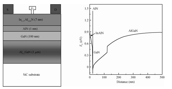
Fig. 1.
Structure and energy band diagram of a schematic InAlN/GaN HEMT with an AlGaN back barrier
SEMICONDUCTOR DEVICES
Bo Liu, Zhihong Feng, Shaobo Dun, Xiongwen Zhang, Guodong Gu, Yuangang Wang, Peng Xu, Zezhao He and Shujun Cai
Corresponding author: Feng Zhihong, Email:blueledviet@yahoo.com.cn
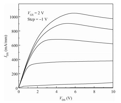
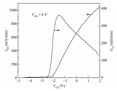
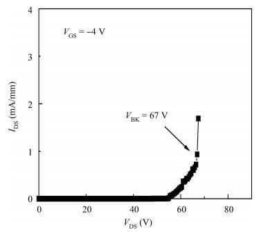
Abstract: We report the DC and RF performance of InAlN/GaN high-electron mobility transistors with AlGaN back barrier grown on SiC substrates. These presented results confirm the high performance that is reachable by InAlN-based technology. The InAlN/GaN HEMT sample showed a high 2DEG mobility of 1550 cm2/(V·s) at a 2DEG density of 1.7×1013 cm-2. DC and RF measurements were performed on the unpassivated device with 0.2 μm "T" gate. The maximum drain current density at VGS=2 V is close to 1.05 A/mm in a reproducible way. The reduction in gate leakage current helps to increase the frequency performance of AlGaN back barrier devices. The power gain cut-off frequency of a transistor with an AlGaN back barrier is 105 GHz, which is much higher than that of the device without an AlGaN back barrier at the same gate length. These results indicate InAlN/GaN HEMT is a promising candidate for millimeter-wave application.
Keywords: AlGaN back barrier, InAlN, high-electron-mobility transistors, power gain cutoff frequency
| [1] |
Feng Z H, Xie S Y, Zhou R, et al. A high-performance enhancement-mode AlGaN/GaN HEMT. Journal of Semiconductors, 2010, 31(8):084001 doi: 10.1088/1674-4926/31/8/084001
|
| [2] |
Ciccognani W, De Dominicis M, Ferrari M, et al. High-power monolithic AlGaN/GaN HEMT switch for X-band applications. IEEE Electron Lett, 2008, 44(55):911
|
| [3] |
Wang Y, Li J Q, Zhang Z G, et al. X-band internally-matched GaN HEMTs. Journal of Semiconductors, 2008, 29(9):1783 http://www.jos.ac.cn/bdtxben/ch/reader/view_abstract.aspx?file_no=08031301&flag=1
|
| [4] |
Feng Z H, Yin J Y, Yuan F P, et al. A 5.1 W/mm power density GaN HEMT on Si substrate. Journal of Semiconductors, 2007, 28(12):1949 http://www.jos.ac.cn/bdtxben/ch/reader/view_abstract.aspx?file_no=07053005&flag=1
|
| [5] |
Wu Y F, Moore M, Saxler A, et al. 40-W/mm double field-plated GaN HEMTs. Proc IEEE Device Res Conf, 2006:151
|
| [6] |
Feng Z H, Zhou R, Xie S Y, et al. 18-GHz 3.65-W/mm enhancement-mode AlGaN/GaN HFET using fluorine plasma ion implantation. IEEE Electron Device Lett, 2010, 31(12):1386 doi: 10.1109/LED.2010.2072901
|
| [7] |
Kuzmik J. Power electronics on InAlN/(In)GaN:prospect for a record performance. IEEE Electron Device Lett, 22(11), 2001:510
|
| [8] |
Liu Bo, Feng Zhihong, Zhang Sen, et al. A 4.69-W/mm output power density InAlN/GaN HEMT grown on sapphire substrate. Journal of Semiconductors, 2011, 32(12):124003 doi: 10.1088/1674-4926/32/12/124003
|
| [9] |
Wang H, Chung J, Gao X, et al. Al2O3 passivated InAlN/GaN HEMTs on SiC substrate with record current density and transconductance. Phys Status Solidi C, 2010, 7(10):2440 doi: 10.1002/pssc.200983899
|
| [10] |
Wang R, Saunier P, Xing X, et al. Gate-recessed enhancement-mode InAlN/AlN/GaN HEMTs with 1.9-A/mm drain current density and 800-mS/mm transconductance. IEEE Electron Device Lett, 2010, 31(12):1383
|
| [11] |
Yue Yuanzheng, Hu Zongyang, Guo Jia, et al. InAlN/AlN/GaN HEMTs with regrown ohmic contacts and fT of 370 GHz. IEEE Electron Device Lett, 2012, 33(7):988 doi: 10.1109/LED.2012.2196751
|
| [12] |
Kuzmik J, Pozzovio G, Ostermaier C, et al. Analysis of degradation mechanisms in lattice-matched InAlN/GaN high-electron-mobility transistors. Jpn J Appl Phys, 2009, 106(12):124503 doi: 10.1063/1.3272058
|
| [13] |
Bahat-Treidel E, Hilt O, Brunner F, et al. Punchthrough-voltage enhancement of AlGaN/GaN HEMTs using AlGaN double-heterojunction confinement. IEEE Trans Electron Devices, 2008, 55(12):3354 doi: 10.1109/TED.2008.2006891
|


Article views: 3164 Times PDF downloads: 26 Times Cited by: 0 Times
Received: 25 September 2012 Revised: 19 November 2012 Online: Published: 01 April 2013
| Citation: |
Bo Liu, Zhihong Feng, Shaobo Dun, Xiongwen Zhang, Guodong Gu, Yuangang Wang, Peng Xu, Zezhao He, Shujun Cai. An extrinsic fmax > 100 GHz InAlN/GaN HEMT with AlGaN back barrier[J]. Journal of Semiconductors, 2013, 34(4): 044006. doi: 10.1088/1674-4926/34/4/044006
****
B Liu, Z H Feng, S B Dun, X W Zhang, G D Gu, Y G Wang, P Xu, Z Z He, S J Cai. An extrinsic fmax > 100 GHz InAlN/GaN HEMT with AlGaN back barrier[J]. J. Semicond., 2013, 34(4): 044006. doi: 10.1088/1674-4926/34/4/044006.

|
| [1] |
Feng Z H, Xie S Y, Zhou R, et al. A high-performance enhancement-mode AlGaN/GaN HEMT. Journal of Semiconductors, 2010, 31(8):084001 doi: 10.1088/1674-4926/31/8/084001
|
| [2] |
Ciccognani W, De Dominicis M, Ferrari M, et al. High-power monolithic AlGaN/GaN HEMT switch for X-band applications. IEEE Electron Lett, 2008, 44(55):911
|
| [3] |
Wang Y, Li J Q, Zhang Z G, et al. X-band internally-matched GaN HEMTs. Journal of Semiconductors, 2008, 29(9):1783 http://www.jos.ac.cn/bdtxben/ch/reader/view_abstract.aspx?file_no=08031301&flag=1
|
| [4] |
Feng Z H, Yin J Y, Yuan F P, et al. A 5.1 W/mm power density GaN HEMT on Si substrate. Journal of Semiconductors, 2007, 28(12):1949 http://www.jos.ac.cn/bdtxben/ch/reader/view_abstract.aspx?file_no=07053005&flag=1
|
| [5] |
Wu Y F, Moore M, Saxler A, et al. 40-W/mm double field-plated GaN HEMTs. Proc IEEE Device Res Conf, 2006:151
|
| [6] |
Feng Z H, Zhou R, Xie S Y, et al. 18-GHz 3.65-W/mm enhancement-mode AlGaN/GaN HFET using fluorine plasma ion implantation. IEEE Electron Device Lett, 2010, 31(12):1386 doi: 10.1109/LED.2010.2072901
|
| [7] |
Kuzmik J. Power electronics on InAlN/(In)GaN:prospect for a record performance. IEEE Electron Device Lett, 22(11), 2001:510
|
| [8] |
Liu Bo, Feng Zhihong, Zhang Sen, et al. A 4.69-W/mm output power density InAlN/GaN HEMT grown on sapphire substrate. Journal of Semiconductors, 2011, 32(12):124003 doi: 10.1088/1674-4926/32/12/124003
|
| [9] |
Wang H, Chung J, Gao X, et al. Al2O3 passivated InAlN/GaN HEMTs on SiC substrate with record current density and transconductance. Phys Status Solidi C, 2010, 7(10):2440 doi: 10.1002/pssc.200983899
|
| [10] |
Wang R, Saunier P, Xing X, et al. Gate-recessed enhancement-mode InAlN/AlN/GaN HEMTs with 1.9-A/mm drain current density and 800-mS/mm transconductance. IEEE Electron Device Lett, 2010, 31(12):1383
|
| [11] |
Yue Yuanzheng, Hu Zongyang, Guo Jia, et al. InAlN/AlN/GaN HEMTs with regrown ohmic contacts and fT of 370 GHz. IEEE Electron Device Lett, 2012, 33(7):988 doi: 10.1109/LED.2012.2196751
|
| [12] |
Kuzmik J, Pozzovio G, Ostermaier C, et al. Analysis of degradation mechanisms in lattice-matched InAlN/GaN high-electron-mobility transistors. Jpn J Appl Phys, 2009, 106(12):124503 doi: 10.1063/1.3272058
|
| [13] |
Bahat-Treidel E, Hilt O, Brunner F, et al. Punchthrough-voltage enhancement of AlGaN/GaN HEMTs using AlGaN double-heterojunction confinement. IEEE Trans Electron Devices, 2008, 55(12):3354 doi: 10.1109/TED.2008.2006891
|

 WeChat ID
Journal of Semiconductors © 2017 All Rights Reserved 京ICP备05085259号-2

 DownLoad:

