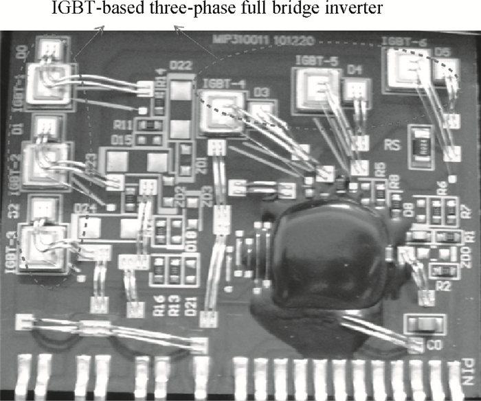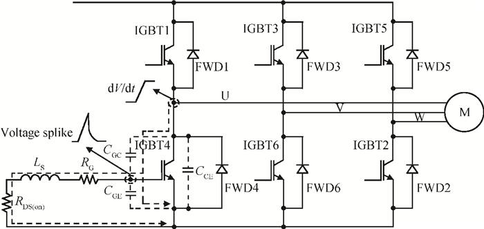
Fig. 1.
Simplified circuit schematic of three-phase full-bridge inverter.
SEMICONDUCTOR INTEGRATED CIRCUITS
Qing Hua1, , Zehong Li1, Bo Zhang1, Xiangjun Huang2 and Dekai Cheng2
Corresponding author: Hua Qing, Email:huaqing2014@126.com
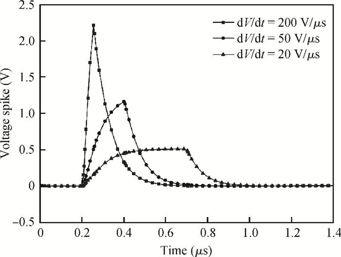
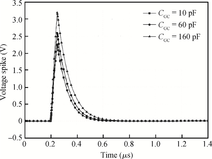
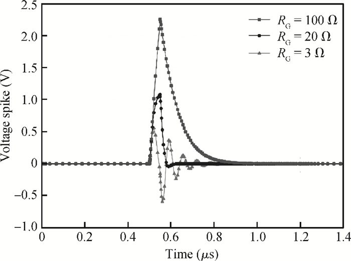
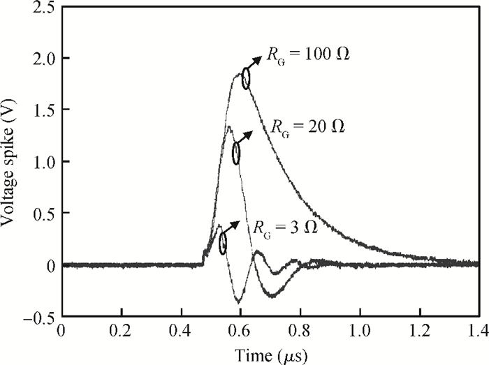
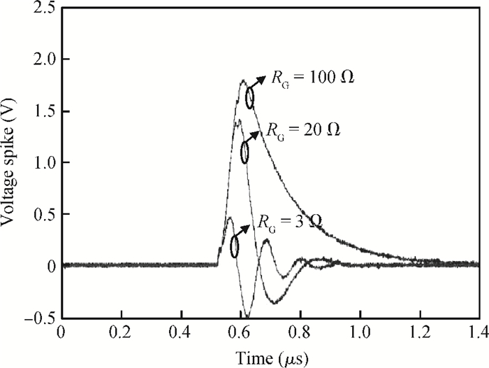
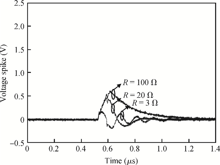
Abstract: The effect of dV/dt on the IGBT gate circuit in IPM is analyzed both by simulation and experiment. It is shown that a voltage slope applied across the collector-emitter terminals of the IGBT can induce a gate voltage spike through the feedback action of the parasitic capacitances of the IGBT. The dV/dt rate, gate-collector capacitance, gate-emitter capacitance and gate resistance have a direct influence on this voltage spike. The device with a higher dV/dt rate, gate-collector capacitance, gate resistance and lower gate-emitter capacitance is more prone to dV/dt induced self turn-on. By optimizing these parameters, the dV/dt induced voltage spike can be effectively controlled.
Keywords: IGBT, dV/dt, voltage spike, IPM
| [1] |
Ranstad P, Nee H P. On dynamic effects influencing IGBT losses in soft-switching converters. IEEE Trans Power Electron, 2011, 26(1):260 doi: 10.1109/TPEL.2010.2055581
|
| [2] |
Letor R, Aniceto G C. Short circuit behavior of IGBT's correlated to the intrinsic device structure and on the application circuit. IEEE Trans Industry Applications, 1995, 31(2):234 doi: 10.1109/28.370268
|
| [3] |
Park S, Jahns T M. Flexible dv/dt and di/dt control method for insulated gate power switches. IEEE Trans Industry Applications, 2003, 39(3):657 doi: 10.1109/TIA.2003.810654
|
| [4] |
Takizawa S, Igarashi S, Kuroki K. A new di/dt control gate drive circuit for IGBTs to reduce EMI noise and switching losses. IEEE PESC, 1998, 2:1443
|
| [5] |
Igarashi S, Takizawa S, Tabata M, et al. An active control gate drive circuit for IGBT's to realize low-noise and snubberless system. Proc ISPSD, 1997:69
|
| [6] |
Bryant A, Yang S, Mawby P, et al. Investigation into IGBT dV/dt during turn-off and its temperature dependence. IEEE Trans Power Electron, 2011, 26(10):3019 doi: 10.1109/TPEL.2011.2125803
|
| [7] |
Idir N, Bausiere R, Franchaud J J. Active gate voltage control of turn-on di/dt and turn-off dv/dt in insulated gate transistors. IEEE Trans Power Electron, 2006, 21(4):849 doi: 10.1109/TPEL.2007.876895
|
| [8] |
Wu W, Held M, Umbricht N, et al. dv/dt induced latching failure in 1200 V/400 A halfbridge IGBT modules. IEEE IRPS, 1994:420 http://ieeexplore.ieee.org/document/307804/?reload=true&arnumber=307804&filter%3DAND(p_IS_Number:7501)
|
| [9] |
Murata K, Harada, K. Analysis of a self turn-on phenomenon on the synchronous rectifier in a DC-DC converter. INTELEC, 2004:199 http://ieeexplore.ieee.org/document/1252113/
|
| [10] |
Yedinak J, Gladish J, Brockway B, et al. A 600 V quick punch through (QPT) IGBT design concept for reducing EMI. Proc ISPSD, 2003:67
|
| [11] |
Musumeci S, Pagano R, Raciti A, et al. A novel protection technique devoted to the improvement of the short circuit ruggedness of IGBTs. IECON, 2003, 2:1733 http://ieeexplore.ieee.org/document/1280319/?arnumber=1280319
|
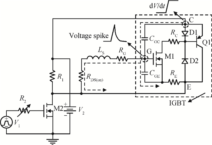
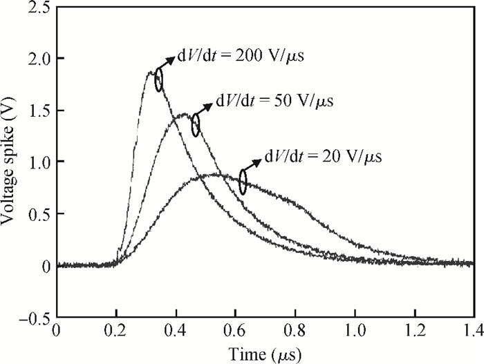
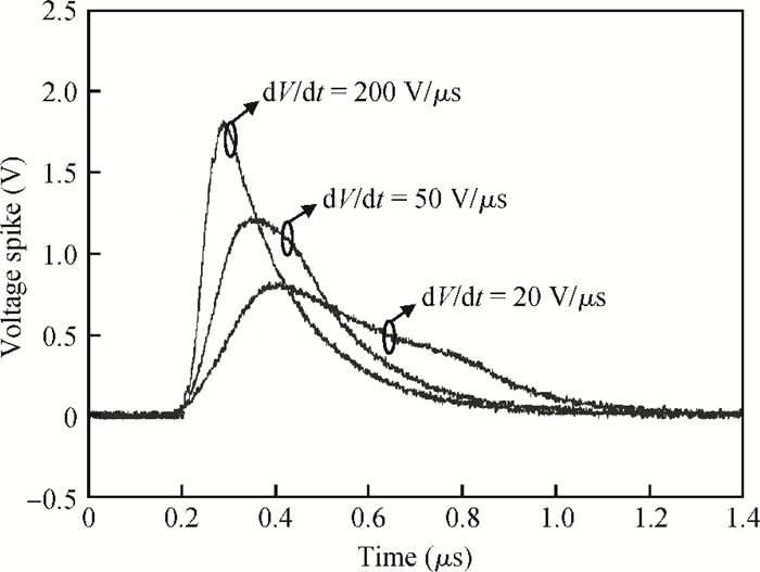
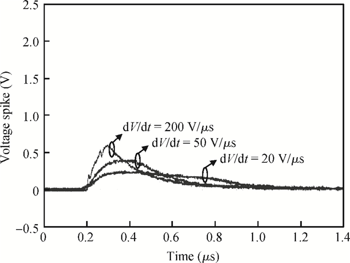
Table 1. Device parameters.

|
| [1] |
Ranstad P, Nee H P. On dynamic effects influencing IGBT losses in soft-switching converters. IEEE Trans Power Electron, 2011, 26(1):260 doi: 10.1109/TPEL.2010.2055581
|
| [2] |
Letor R, Aniceto G C. Short circuit behavior of IGBT's correlated to the intrinsic device structure and on the application circuit. IEEE Trans Industry Applications, 1995, 31(2):234 doi: 10.1109/28.370268
|
| [3] |
Park S, Jahns T M. Flexible dv/dt and di/dt control method for insulated gate power switches. IEEE Trans Industry Applications, 2003, 39(3):657 doi: 10.1109/TIA.2003.810654
|
| [4] |
Takizawa S, Igarashi S, Kuroki K. A new di/dt control gate drive circuit for IGBTs to reduce EMI noise and switching losses. IEEE PESC, 1998, 2:1443
|
| [5] |
Igarashi S, Takizawa S, Tabata M, et al. An active control gate drive circuit for IGBT's to realize low-noise and snubberless system. Proc ISPSD, 1997:69
|
| [6] |
Bryant A, Yang S, Mawby P, et al. Investigation into IGBT dV/dt during turn-off and its temperature dependence. IEEE Trans Power Electron, 2011, 26(10):3019 doi: 10.1109/TPEL.2011.2125803
|
| [7] |
Idir N, Bausiere R, Franchaud J J. Active gate voltage control of turn-on di/dt and turn-off dv/dt in insulated gate transistors. IEEE Trans Power Electron, 2006, 21(4):849 doi: 10.1109/TPEL.2007.876895
|
| [8] |
Wu W, Held M, Umbricht N, et al. dv/dt induced latching failure in 1200 V/400 A halfbridge IGBT modules. IEEE IRPS, 1994:420 http://ieeexplore.ieee.org/document/307804/?reload=true&arnumber=307804&filter%3DAND(p_IS_Number:7501)
|
| [9] |
Murata K, Harada, K. Analysis of a self turn-on phenomenon on the synchronous rectifier in a DC-DC converter. INTELEC, 2004:199 http://ieeexplore.ieee.org/document/1252113/
|
| [10] |
Yedinak J, Gladish J, Brockway B, et al. A 600 V quick punch through (QPT) IGBT design concept for reducing EMI. Proc ISPSD, 2003:67
|
| [11] |
Musumeci S, Pagano R, Raciti A, et al. A novel protection technique devoted to the improvement of the short circuit ruggedness of IGBTs. IECON, 2003, 2:1733 http://ieeexplore.ieee.org/document/1280319/?arnumber=1280319
|


Article views: 4230 Times PDF downloads: 142 Times Cited by: 0 Times
Received: 13 August 2012 Revised: 23 October 2012 Online: Published: 01 April 2013
| Citation: |
Qing Hua, Zehong Li, Bo Zhang, Xiangjun Huang, Dekai Cheng. Analysis of the dV/dt effect on an IGBT gate circuit in IPM[J]. Journal of Semiconductors, 2013, 34(4): 045001. doi: 10.1088/1674-4926/34/4/045001
****
Q Hua, Z H Li, B Zhang, X J Huang, D K Cheng. Analysis of the dV/dt effect on an IGBT gate circuit in IPM[J]. J. Semicond., 2013, 34(4): 045001. doi: 10.1088/1674-4926/34/4/045001.

|
| [1] |
Ranstad P, Nee H P. On dynamic effects influencing IGBT losses in soft-switching converters. IEEE Trans Power Electron, 2011, 26(1):260 doi: 10.1109/TPEL.2010.2055581
|
| [2] |
Letor R, Aniceto G C. Short circuit behavior of IGBT's correlated to the intrinsic device structure and on the application circuit. IEEE Trans Industry Applications, 1995, 31(2):234 doi: 10.1109/28.370268
|
| [3] |
Park S, Jahns T M. Flexible dv/dt and di/dt control method for insulated gate power switches. IEEE Trans Industry Applications, 2003, 39(3):657 doi: 10.1109/TIA.2003.810654
|
| [4] |
Takizawa S, Igarashi S, Kuroki K. A new di/dt control gate drive circuit for IGBTs to reduce EMI noise and switching losses. IEEE PESC, 1998, 2:1443
|
| [5] |
Igarashi S, Takizawa S, Tabata M, et al. An active control gate drive circuit for IGBT's to realize low-noise and snubberless system. Proc ISPSD, 1997:69
|
| [6] |
Bryant A, Yang S, Mawby P, et al. Investigation into IGBT dV/dt during turn-off and its temperature dependence. IEEE Trans Power Electron, 2011, 26(10):3019 doi: 10.1109/TPEL.2011.2125803
|
| [7] |
Idir N, Bausiere R, Franchaud J J. Active gate voltage control of turn-on di/dt and turn-off dv/dt in insulated gate transistors. IEEE Trans Power Electron, 2006, 21(4):849 doi: 10.1109/TPEL.2007.876895
|
| [8] |
Wu W, Held M, Umbricht N, et al. dv/dt induced latching failure in 1200 V/400 A halfbridge IGBT modules. IEEE IRPS, 1994:420 http://ieeexplore.ieee.org/document/307804/?reload=true&arnumber=307804&filter%3DAND(p_IS_Number:7501)
|
| [9] |
Murata K, Harada, K. Analysis of a self turn-on phenomenon on the synchronous rectifier in a DC-DC converter. INTELEC, 2004:199 http://ieeexplore.ieee.org/document/1252113/
|
| [10] |
Yedinak J, Gladish J, Brockway B, et al. A 600 V quick punch through (QPT) IGBT design concept for reducing EMI. Proc ISPSD, 2003:67
|
| [11] |
Musumeci S, Pagano R, Raciti A, et al. A novel protection technique devoted to the improvement of the short circuit ruggedness of IGBTs. IECON, 2003, 2:1733 http://ieeexplore.ieee.org/document/1280319/?arnumber=1280319
|

 WeChat ID
Journal of Semiconductors © 2017 All Rights Reserved 京ICP备05085259号-2

 DownLoad: