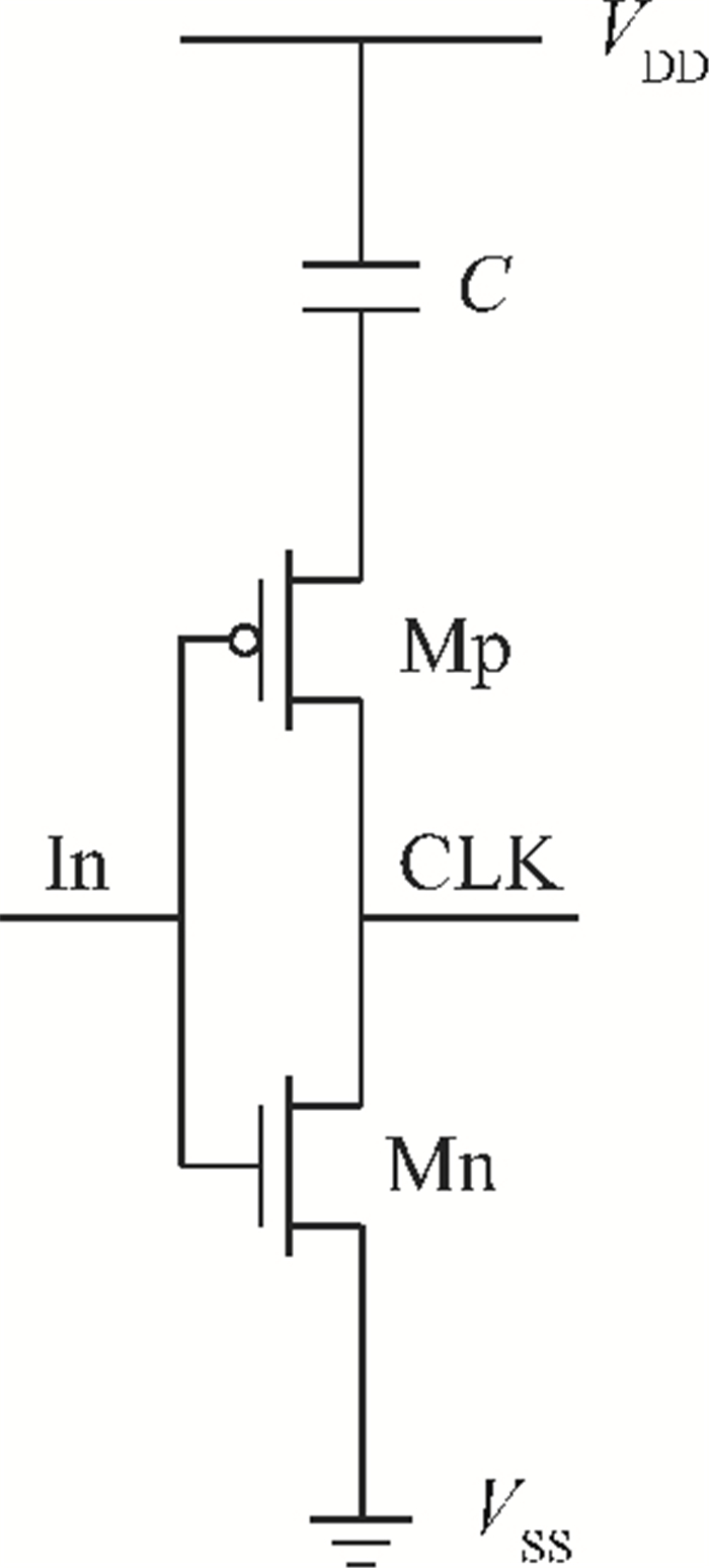
Fig. 1.
(a) Schematic of a traditional RC triggered ESD circuit and (b) waveforms of node voltages and current.
SEMICONDUCTOR INTEGRATED CIRCUITS
Zhaonian Yang, Hongxia Liu and Shulong Wang
Corresponding author: Yang Zhaonian, Email:e_yangzhaonian@sina.com
Abstract: An electrostatic discharge (ESD) detection circuit with a modified RC network for a 90-nm process clamp circuit is proposed. The leakage current is reduced to 4.6 nA at 25℃. Under the ESD event, it injects a 38.7 mA trigger current into the P-substrate to trigger SCR, and SCR can be turned on the discharge of the ESD energy. The capacitor area used is only 4.2 μm2. The simulation result shows that the proposed circuit can save power consumption and layout area when achieving the same trigger efficiency, compared with the previous circuits.
Key words: clamp circuit, electrostatic discharge, leakage current, RC network
| [1] |
Voldman S. ESD:circuits and devices. New York:Wiley, 2006
|
| [2] |
Joshi G, Singh D, Thangjam S. Effect of temperature variation on gate tunneling currents in nanoscale MOSFETs. Proc IEEE Conf Nanotechnology, 2008:37 http://ieeexplore.ieee.org/document/4617001/keywords
|
| [3] |
Datta S, Dewey G, Doczy M, et al. High mobility Si/SiGe strained channel MOS transistors with HfO2/TiN gate stack. IEDM Tech Dig, 2003:653
|
| [4] |
Hong S, Shim K, Yang J. Reduced gate leakage current in AlGaN/GaN HEMT by oxygen passivation of AlGaN surface. Electron Lett, 2008, 44:1091 doi: 10.1049/el:20081350
|
| [5] |
Altolaguirre F A, Ker M D. Overview on the design of low-leakage power-rail ESD clamp circuits in nanoscale CMOS processes. Argentine School of Micro-Nanoelectronics Technology and Applications (EAMTA), 2011:1 http://ieeexplore.ieee.org/document/6021283/keywords
|
| [6] |
Ker M D. Whole-chip ESD protection design with efficient VDD-to-VSS ESD clamp circuits for submicron CMOS VLSI. IEEE Trans Electron Devices, 1999, 46:173 doi: 10.1109/16.737457
|
| [7] |
Sarro J D, Chatty K, Gauthier R, et al. Evaluation of SCR-based ESD protection devices in 90-nm and 65-nm CMOS technologies. Proc IEEE Int Reliability Physics Symp, 2007:348
|
| [8] |
Smith J C, Cline R, Boselli G. A low leakage low cost PMOS-based power supply clamp with active feedback for ESD protection in 65-nm CMOS technologies. Proc EOS/ESD Symp, 2005:298 http://ieeexplore.ieee.org/document/05271748/
|
| [9] |
Ker M D, Chiu P Y, Tsai F Y, et al. On the design of power-rail ESD clamp circuit with consideration of gate leakage current in 65-nm low-voltage CMOS process. Proc IEEE Int Symp Circuits Syst, 2009:2281 http://ieeexplore.ieee.org/document/5118254/
|
| [10] |
Chiu P Y, Ker M D, Tsai F Y, et al. Ultra-low-leakage power-rail ESD clamp circuit in nanoscale low-voltage CMOS process. Proc IEEE Int Reliability Physics Symp, 2009:750 http://ieeexplore.ieee.org/document/5173343/authors
|
| [11] |
Wang C T, Ker M D. Design of power-rail ESD clamp circuit with ultra-low standby leakage current in nanoscale CMOS technology. IEEE J Solid-State Circuits, 2009, 44:956 doi: 10.1109/JSSC.2008.2012372
|
| [12] |
Chiu P Y, Ker M D. New low-leakage power-rail ESD clamp circuit in a 65-nm low-voltage CMOS process. IEEE Trans Device Mater Reliab, 2011, 11:474 doi: 10.1109/TDMR.2010.2066976
|
| [13] |
Wang C T, Ker M D. Design of 2×VDD-tolerant power-rail ESD clamp circuit with consideration of gate leakage current in 65-nm CMOS technology. IEEE Trans Electron Devices, 2010, 57:1460 doi: 10.1109/TED.2010.2046457
|
| [14] |
Yeh C T, Ker M D. New design of 2×VDD-tolerant power-rail ESD clamp circuit for mixed-voltage I/O buffers in 65-nm CMOS technology. IEEE Trans Circuits Syst Ⅱ, Express Briefs, 2012, 59:178 doi: 10.1109/TCSII.2012.2184372
|
| [15] |
Smith J C, Boselli G. A MOSFET power supply clamp with feedback enhanced triggering for ESD protection in advanced CMOS technologies. Microelectron Reliab, 2005, 45:201 doi: 10.1016/j.microrel.2004.05.008
|
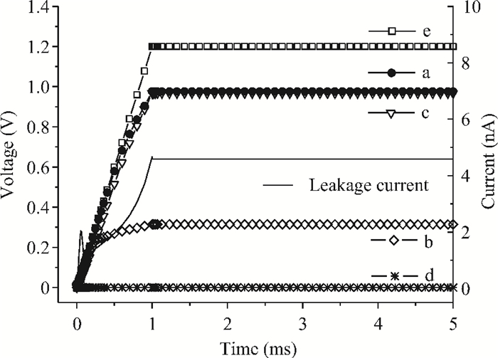
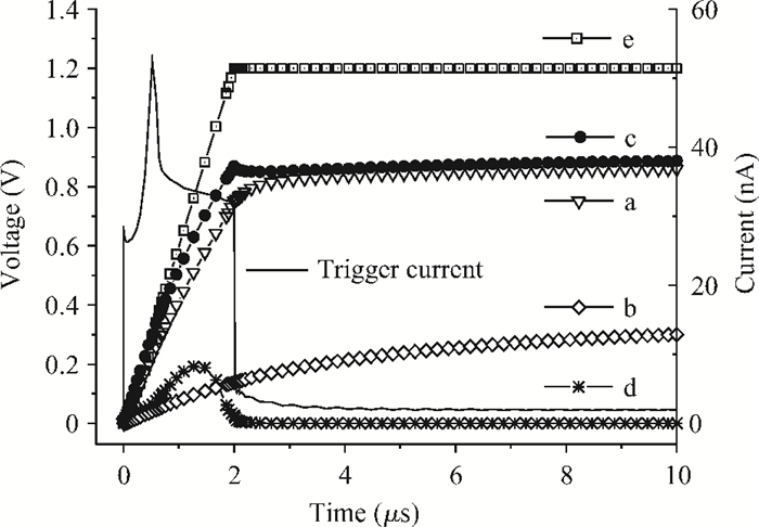
Table 1.
Dimensions of the devices in the proposed circuit. Unit:

|
Table 2. Key parameters of the three circuits.

|
Table 3. Leakage currents under different conditions. Unit: nA

|
| [1] |
Voldman S. ESD:circuits and devices. New York:Wiley, 2006
|
| [2] |
Joshi G, Singh D, Thangjam S. Effect of temperature variation on gate tunneling currents in nanoscale MOSFETs. Proc IEEE Conf Nanotechnology, 2008:37 http://ieeexplore.ieee.org/document/4617001/keywords
|
| [3] |
Datta S, Dewey G, Doczy M, et al. High mobility Si/SiGe strained channel MOS transistors with HfO2/TiN gate stack. IEDM Tech Dig, 2003:653
|
| [4] |
Hong S, Shim K, Yang J. Reduced gate leakage current in AlGaN/GaN HEMT by oxygen passivation of AlGaN surface. Electron Lett, 2008, 44:1091 doi: 10.1049/el:20081350
|
| [5] |
Altolaguirre F A, Ker M D. Overview on the design of low-leakage power-rail ESD clamp circuits in nanoscale CMOS processes. Argentine School of Micro-Nanoelectronics Technology and Applications (EAMTA), 2011:1 http://ieeexplore.ieee.org/document/6021283/keywords
|
| [6] |
Ker M D. Whole-chip ESD protection design with efficient VDD-to-VSS ESD clamp circuits for submicron CMOS VLSI. IEEE Trans Electron Devices, 1999, 46:173 doi: 10.1109/16.737457
|
| [7] |
Sarro J D, Chatty K, Gauthier R, et al. Evaluation of SCR-based ESD protection devices in 90-nm and 65-nm CMOS technologies. Proc IEEE Int Reliability Physics Symp, 2007:348
|
| [8] |
Smith J C, Cline R, Boselli G. A low leakage low cost PMOS-based power supply clamp with active feedback for ESD protection in 65-nm CMOS technologies. Proc EOS/ESD Symp, 2005:298 http://ieeexplore.ieee.org/document/05271748/
|
| [9] |
Ker M D, Chiu P Y, Tsai F Y, et al. On the design of power-rail ESD clamp circuit with consideration of gate leakage current in 65-nm low-voltage CMOS process. Proc IEEE Int Symp Circuits Syst, 2009:2281 http://ieeexplore.ieee.org/document/5118254/
|
| [10] |
Chiu P Y, Ker M D, Tsai F Y, et al. Ultra-low-leakage power-rail ESD clamp circuit in nanoscale low-voltage CMOS process. Proc IEEE Int Reliability Physics Symp, 2009:750 http://ieeexplore.ieee.org/document/5173343/authors
|
| [11] |
Wang C T, Ker M D. Design of power-rail ESD clamp circuit with ultra-low standby leakage current in nanoscale CMOS technology. IEEE J Solid-State Circuits, 2009, 44:956 doi: 10.1109/JSSC.2008.2012372
|
| [12] |
Chiu P Y, Ker M D. New low-leakage power-rail ESD clamp circuit in a 65-nm low-voltage CMOS process. IEEE Trans Device Mater Reliab, 2011, 11:474 doi: 10.1109/TDMR.2010.2066976
|
| [13] |
Wang C T, Ker M D. Design of 2×VDD-tolerant power-rail ESD clamp circuit with consideration of gate leakage current in 65-nm CMOS technology. IEEE Trans Electron Devices, 2010, 57:1460 doi: 10.1109/TED.2010.2046457
|
| [14] |
Yeh C T, Ker M D. New design of 2×VDD-tolerant power-rail ESD clamp circuit for mixed-voltage I/O buffers in 65-nm CMOS technology. IEEE Trans Circuits Syst Ⅱ, Express Briefs, 2012, 59:178 doi: 10.1109/TCSII.2012.2184372
|
| [15] |
Smith J C, Boselli G. A MOSFET power supply clamp with feedback enhanced triggering for ESD protection in advanced CMOS technologies. Microelectron Reliab, 2005, 45:201 doi: 10.1016/j.microrel.2004.05.008
|


Article views: 3741 Times PDF downloads: 58 Times Cited by: 0 Times
Received: 12 September 2012 Revised: 12 October 2012 Online: Published: 01 April 2013
| Citation: |
Zhaonian Yang, Hongxia Liu, Shulong Wang. A low leakage power-rail ESD detection circuit with a modified RC network for a 90-nm CMOS process[J]. Journal of Semiconductors, 2013, 34(4): 045010. doi: 10.1088/1674-4926/34/4/045010
****
Z N Yang, H X Liu, S L Wang. A low leakage power-rail ESD detection circuit with a modified RC network for a 90-nm CMOS process[J]. J. Semicond., 2013, 34(4): 045010. doi: 10.1088/1674-4926/34/4/045010.

|
| [1] |
Voldman S. ESD:circuits and devices. New York:Wiley, 2006
|
| [2] |
Joshi G, Singh D, Thangjam S. Effect of temperature variation on gate tunneling currents in nanoscale MOSFETs. Proc IEEE Conf Nanotechnology, 2008:37 http://ieeexplore.ieee.org/document/4617001/keywords
|
| [3] |
Datta S, Dewey G, Doczy M, et al. High mobility Si/SiGe strained channel MOS transistors with HfO2/TiN gate stack. IEDM Tech Dig, 2003:653
|
| [4] |
Hong S, Shim K, Yang J. Reduced gate leakage current in AlGaN/GaN HEMT by oxygen passivation of AlGaN surface. Electron Lett, 2008, 44:1091 doi: 10.1049/el:20081350
|
| [5] |
Altolaguirre F A, Ker M D. Overview on the design of low-leakage power-rail ESD clamp circuits in nanoscale CMOS processes. Argentine School of Micro-Nanoelectronics Technology and Applications (EAMTA), 2011:1 http://ieeexplore.ieee.org/document/6021283/keywords
|
| [6] |
Ker M D. Whole-chip ESD protection design with efficient VDD-to-VSS ESD clamp circuits for submicron CMOS VLSI. IEEE Trans Electron Devices, 1999, 46:173 doi: 10.1109/16.737457
|
| [7] |
Sarro J D, Chatty K, Gauthier R, et al. Evaluation of SCR-based ESD protection devices in 90-nm and 65-nm CMOS technologies. Proc IEEE Int Reliability Physics Symp, 2007:348
|
| [8] |
Smith J C, Cline R, Boselli G. A low leakage low cost PMOS-based power supply clamp with active feedback for ESD protection in 65-nm CMOS technologies. Proc EOS/ESD Symp, 2005:298 http://ieeexplore.ieee.org/document/05271748/
|
| [9] |
Ker M D, Chiu P Y, Tsai F Y, et al. On the design of power-rail ESD clamp circuit with consideration of gate leakage current in 65-nm low-voltage CMOS process. Proc IEEE Int Symp Circuits Syst, 2009:2281 http://ieeexplore.ieee.org/document/5118254/
|
| [10] |
Chiu P Y, Ker M D, Tsai F Y, et al. Ultra-low-leakage power-rail ESD clamp circuit in nanoscale low-voltage CMOS process. Proc IEEE Int Reliability Physics Symp, 2009:750 http://ieeexplore.ieee.org/document/5173343/authors
|
| [11] |
Wang C T, Ker M D. Design of power-rail ESD clamp circuit with ultra-low standby leakage current in nanoscale CMOS technology. IEEE J Solid-State Circuits, 2009, 44:956 doi: 10.1109/JSSC.2008.2012372
|
| [12] |
Chiu P Y, Ker M D. New low-leakage power-rail ESD clamp circuit in a 65-nm low-voltage CMOS process. IEEE Trans Device Mater Reliab, 2011, 11:474 doi: 10.1109/TDMR.2010.2066976
|
| [13] |
Wang C T, Ker M D. Design of 2×VDD-tolerant power-rail ESD clamp circuit with consideration of gate leakage current in 65-nm CMOS technology. IEEE Trans Electron Devices, 2010, 57:1460 doi: 10.1109/TED.2010.2046457
|
| [14] |
Yeh C T, Ker M D. New design of 2×VDD-tolerant power-rail ESD clamp circuit for mixed-voltage I/O buffers in 65-nm CMOS technology. IEEE Trans Circuits Syst Ⅱ, Express Briefs, 2012, 59:178 doi: 10.1109/TCSII.2012.2184372
|
| [15] |
Smith J C, Boselli G. A MOSFET power supply clamp with feedback enhanced triggering for ESD protection in advanced CMOS technologies. Microelectron Reliab, 2005, 45:201 doi: 10.1016/j.microrel.2004.05.008
|

 WeChat ID
Journal of Semiconductors © 2017 All Rights Reserved 京ICP备05085259号-2

 DownLoad: