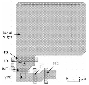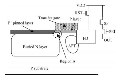
Fig. 1.
Typical structure of a 4-T CMOS image sensor.
SEMICONDUCTOR DEVICES
Liqiang Han, Suying Yao, Jiangtao Xu, Chao Xu and Zhiyuan Gao
Corresponding author: Xu Jiangtao, Email:xujiangtao@tju.edu.cn
Abstract: A method to judge complete charger transfer is proposed for a four-transistor CMOS image sensor with a large pixel size. Based on the emission current theory, a qualitative photoresponse model is established to the preliminary prediction. Further analysis of noise for incomplete charge transfer predicts the noise variation. The test pixels were fabricated in a specialized 0.18 μ m CMOS image sensor process and two different processes of buried N layer implantation are compared. The trend prediction corresponds with the test results, especially as it can distinguish an unobvious incomplete charge transfer. The method helps us judge whether the charge transfer time satisfies the requirements of the readout circuit for the given process especially for pixels of a large size.
Keywords: CMOS image sensor, charge transfer, pinned photodiode, nonlinearity, shot noise
| [1] |
Teranishi N, Kohono A, Ishihara Y, et al. No image lag photodiode structure in the interline CCD image sensor. International Electron Devices Meeting, 1982:324 http://ericfossum.com/Publications/Papers/2014%20JEDS%20Review%20of%20the%20PPD.pdf
|
| [2] |
Lee P P, Guidash R M, Stevens E G, et al. Active pixel sensor integrated with a pinned photodiode. USA Patent, No.5625210, 1997
|
| [3] |
Li Weiping, Xu Jiangtao, Xu Chao, et al. Collection efficiency and charge transfer optimization for a 4-T pixel with multi N-type implants. Journal of Semiconductors, 2011, 32(12):124008 doi: 10.1088/1674-4926/32/12/124008
|
| [4] |
Wang Xinyang. Noise in sub-micron CMOS image sensors. PhD Dissertation, Delft University, 2008 https://repository.tudelft.nl/islandora/object/uuid:2f31c7c5-5019-4cab-a9c5-65528f886a76/datastream/OBJ
|
| [5] |
Michelot J, Roy F, Prima J, et al. Back illuminated vertically pinned photodiode with in depth charge storage. International Image Sensor Workshop, 2011 http://www.docin.com/p-674165012.html
|
| [6] |
Yeh S F, Hsieh C C, Chiu C F, et al. An image lag free CMOS image sensor with constant-residue reset. International Symposium on VLSI Design, Automation and Test, 2011:1
|
| [7] |
Fossum E R. Charge transfer noise and lag in CMOS active pixel sensors. IEEE Workshop on CCDs and Advanced Image Sensors, 2003 http://ericfossum.com/Publications/Papers/Noise%20in%20Charge%20Transfer%20for%20Workshop.pdf
|
| [8] |
Fowler B, Liu X. Charge transfer noise in image sensors. International Image Sensor Workshop, 2007
|
| [9] |
Liu X, Fowler B, Do H, et al. High performance CMOS image sensor for low light imaging. International Image Sensor Workshop, 2007 http://citeseerx.ist.psu.edu/viewdoc/summary?doi=10.1.1.516.3950
|
| [10] |
Ramaswami S, Agwani S, Loh L, et al. Characterization of pixel response time and image lag in CMOS sensors. IEEE Workshop on CCDs and Advanced Image Sensors, 2001
|
| [11] |
Ohta J. Smart CMOS image sensors and applications. New York:CRC Press Taylor & Francis Group, 2008 doi: 10.1201/9781420019155.ch5
|
| [12] |
Janesick J R. Photon transfer DN→λ. Bellingham:SPIE Press, 2007 http://astro.cornell.edu/academics/courses/astro3310/Books/Janesick_PhotonTransfer_SPIE1987.pdf
|
| [13] |
Pain B, Yang G, Ortiz M, et al. Analysis and enhancement of low-light-level performance of photodiode-type CMOS active pixel imagers operated with sub-threshold reset. IEEE Workshop on CCDs and Advanced Image Sensors, 1999 https://trs.jpl.nasa.gov/handle/2014/17488
|
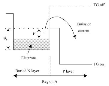
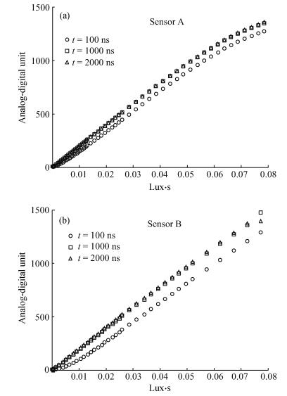
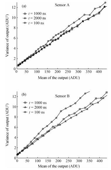
Table 1. Parameters of buried N layer implantation.

|
Table 2. Main performance parameters of the test pixels.

|
| [1] |
Teranishi N, Kohono A, Ishihara Y, et al. No image lag photodiode structure in the interline CCD image sensor. International Electron Devices Meeting, 1982:324 http://ericfossum.com/Publications/Papers/2014%20JEDS%20Review%20of%20the%20PPD.pdf
|
| [2] |
Lee P P, Guidash R M, Stevens E G, et al. Active pixel sensor integrated with a pinned photodiode. USA Patent, No.5625210, 1997
|
| [3] |
Li Weiping, Xu Jiangtao, Xu Chao, et al. Collection efficiency and charge transfer optimization for a 4-T pixel with multi N-type implants. Journal of Semiconductors, 2011, 32(12):124008 doi: 10.1088/1674-4926/32/12/124008
|
| [4] |
Wang Xinyang. Noise in sub-micron CMOS image sensors. PhD Dissertation, Delft University, 2008 https://repository.tudelft.nl/islandora/object/uuid:2f31c7c5-5019-4cab-a9c5-65528f886a76/datastream/OBJ
|
| [5] |
Michelot J, Roy F, Prima J, et al. Back illuminated vertically pinned photodiode with in depth charge storage. International Image Sensor Workshop, 2011 http://www.docin.com/p-674165012.html
|
| [6] |
Yeh S F, Hsieh C C, Chiu C F, et al. An image lag free CMOS image sensor with constant-residue reset. International Symposium on VLSI Design, Automation and Test, 2011:1
|
| [7] |
Fossum E R. Charge transfer noise and lag in CMOS active pixel sensors. IEEE Workshop on CCDs and Advanced Image Sensors, 2003 http://ericfossum.com/Publications/Papers/Noise%20in%20Charge%20Transfer%20for%20Workshop.pdf
|
| [8] |
Fowler B, Liu X. Charge transfer noise in image sensors. International Image Sensor Workshop, 2007
|
| [9] |
Liu X, Fowler B, Do H, et al. High performance CMOS image sensor for low light imaging. International Image Sensor Workshop, 2007 http://citeseerx.ist.psu.edu/viewdoc/summary?doi=10.1.1.516.3950
|
| [10] |
Ramaswami S, Agwani S, Loh L, et al. Characterization of pixel response time and image lag in CMOS sensors. IEEE Workshop on CCDs and Advanced Image Sensors, 2001
|
| [11] |
Ohta J. Smart CMOS image sensors and applications. New York:CRC Press Taylor & Francis Group, 2008 doi: 10.1201/9781420019155.ch5
|
| [12] |
Janesick J R. Photon transfer DN→λ. Bellingham:SPIE Press, 2007 http://astro.cornell.edu/academics/courses/astro3310/Books/Janesick_PhotonTransfer_SPIE1987.pdf
|
| [13] |
Pain B, Yang G, Ortiz M, et al. Analysis and enhancement of low-light-level performance of photodiode-type CMOS active pixel imagers operated with sub-threshold reset. IEEE Workshop on CCDs and Advanced Image Sensors, 1999 https://trs.jpl.nasa.gov/handle/2014/17488
|


Article views: 4223 Times PDF downloads: 127 Times Cited by: 0 Times
Received: 29 July 2012 Revised: 28 September 2012 Online: Published: 01 May 2013
| Citation: |
Liqiang Han, Suying Yao, Jiangtao Xu, Chao Xu, Zhiyuan Gao. Analysis of incomplete charge transfer effects in a CMOS image sensor[J]. Journal of Semiconductors, 2013, 34(5): 054009. doi: 10.1088/1674-4926/34/5/054009
****
L Q Han, S Y Yao, J T Xu, C Xu, Z Y Gao. Analysis of incomplete charge transfer effects in a CMOS image sensor[J]. J. Semicond., 2013, 34(5): 054009. doi: 10.1088/1674-4926/34/5/054009.

|
| [1] |
Teranishi N, Kohono A, Ishihara Y, et al. No image lag photodiode structure in the interline CCD image sensor. International Electron Devices Meeting, 1982:324 http://ericfossum.com/Publications/Papers/2014%20JEDS%20Review%20of%20the%20PPD.pdf
|
| [2] |
Lee P P, Guidash R M, Stevens E G, et al. Active pixel sensor integrated with a pinned photodiode. USA Patent, No.5625210, 1997
|
| [3] |
Li Weiping, Xu Jiangtao, Xu Chao, et al. Collection efficiency and charge transfer optimization for a 4-T pixel with multi N-type implants. Journal of Semiconductors, 2011, 32(12):124008 doi: 10.1088/1674-4926/32/12/124008
|
| [4] |
Wang Xinyang. Noise in sub-micron CMOS image sensors. PhD Dissertation, Delft University, 2008 https://repository.tudelft.nl/islandora/object/uuid:2f31c7c5-5019-4cab-a9c5-65528f886a76/datastream/OBJ
|
| [5] |
Michelot J, Roy F, Prima J, et al. Back illuminated vertically pinned photodiode with in depth charge storage. International Image Sensor Workshop, 2011 http://www.docin.com/p-674165012.html
|
| [6] |
Yeh S F, Hsieh C C, Chiu C F, et al. An image lag free CMOS image sensor with constant-residue reset. International Symposium on VLSI Design, Automation and Test, 2011:1
|
| [7] |
Fossum E R. Charge transfer noise and lag in CMOS active pixel sensors. IEEE Workshop on CCDs and Advanced Image Sensors, 2003 http://ericfossum.com/Publications/Papers/Noise%20in%20Charge%20Transfer%20for%20Workshop.pdf
|
| [8] |
Fowler B, Liu X. Charge transfer noise in image sensors. International Image Sensor Workshop, 2007
|
| [9] |
Liu X, Fowler B, Do H, et al. High performance CMOS image sensor for low light imaging. International Image Sensor Workshop, 2007 http://citeseerx.ist.psu.edu/viewdoc/summary?doi=10.1.1.516.3950
|
| [10] |
Ramaswami S, Agwani S, Loh L, et al. Characterization of pixel response time and image lag in CMOS sensors. IEEE Workshop on CCDs and Advanced Image Sensors, 2001
|
| [11] |
Ohta J. Smart CMOS image sensors and applications. New York:CRC Press Taylor & Francis Group, 2008 doi: 10.1201/9781420019155.ch5
|
| [12] |
Janesick J R. Photon transfer DN→λ. Bellingham:SPIE Press, 2007 http://astro.cornell.edu/academics/courses/astro3310/Books/Janesick_PhotonTransfer_SPIE1987.pdf
|
| [13] |
Pain B, Yang G, Ortiz M, et al. Analysis and enhancement of low-light-level performance of photodiode-type CMOS active pixel imagers operated with sub-threshold reset. IEEE Workshop on CCDs and Advanced Image Sensors, 1999 https://trs.jpl.nasa.gov/handle/2014/17488
|

 WeChat ID
Journal of Semiconductors © 2017 All Rights Reserved 京ICP备05085259号-2

 DownLoad: