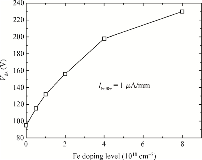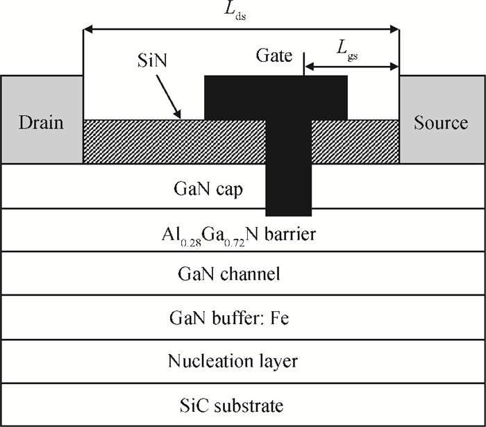
Fig. 1.
Schematic cross section of the developed GaN HEMTs.
SEMICONDUCTOR DEVICES
Chunjiang Ren, Zhonghui Li, Xuming Yu, Quanhui Wang, Wen Wang, Tangsheng Chen and Bin Zhang
Corresponding author: Ren Chunjiang, Email:rencj2010@tom.com
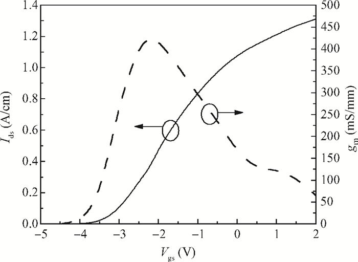
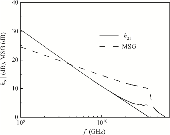
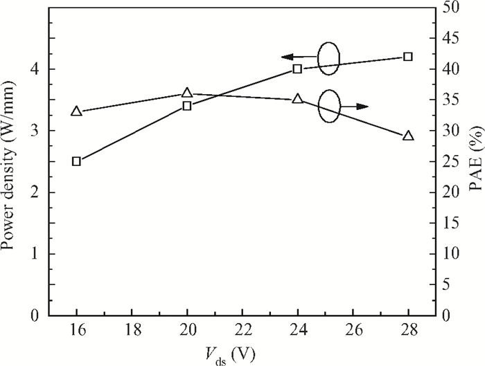
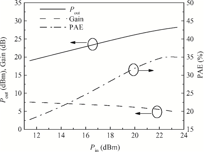
Abstract: SiN dielectrically-defined 0.15 μm field plated GaN HEMTs for millimeter-wave application have been presented. The AlGaN/GaN hetero-structure epitaxial material for HEMTs fabrication was grown on a 3-inch SiC substrate with an Fe doped GaN buffer layer by metal-organic chemical deposition. Electron beam lithography was used to define both the gate footprint and the cap of the gate with an integrated field plate. Gate recessing was performed to control the threshold voltage of the devices. The fabricated GaN HEMTs exhibited a unit current gain cut-off frequency of 39 GHz and a maximum frequency of oscillation of 63 GHz. Load-pull measurements carried out at 35 GHz showed a power density of 4 W/mm with associated power gain and power added efficiency of 5.3 dB and 35%, respectively, for a 0.15 mm gate width device operated at a 24 V drain bias. The developed 0.15 μm gate length GaN HEMT technology is suitable for Ka band applications and is ready for millimeter-wave power MMICs development.
Keywords: AlGaN/GaN, HEMT, Ohmic contact, ICP etching, field plate, millimeter-wave application
| [1] |
Micovic M, Nguyen N X, Janke E, et al. GaN/AlGaN high electron mobility transistor with fT of 110 GHz. Electron Lett, 2000, 36(4):358 doi: 10.1049/el:20000296
|
| [2] |
Inoue T, Ando Y, Kasahara K, et al. Advanced RF characterization and delay-time analysis of short channel AlGaN/GaN heterojunction FETs. IEICE Trans Electron, 2003, Eg6-C(10):2065 http://ci.nii.ac.jp/naid/110003214508
|
| [3] |
Wu Y F, Moor M, Saxler A, et al. 3.5-Watt AlGaN/GaN HEMTs and amplifiers at 35 GHz. IEDM Technical Digest, 2003:579 http://ieeexplore.ieee.org/document/1269349/
|
| [4] |
Inoue T, Ando Y, Miyamoto H, et al. 30 GHz-band 5.8 W high-power AlGaN/GaN heterojunction-FET. IEEE MTT-S Digest, 2004:1649
|
| [5] |
Palacios T, Chakraborty A, Rajan S, et al. High-power AlGaN/GaN HEMTs for Ka-band applications. IEEE Electron Device Lett, 2005, 26(11):781 doi: 10.1109/LED.2005.857701
|
| [6] |
Wu Y F, Moor M, Abrahamsen A, et al. High-voltage millimeter-wave GaN HEMTs with 13.7 W/mm power density. IEEE Compound Semiconductor Integrated circuits Conference, 2007:405 http://ieeexplore.ieee.org/document/4418958/?arnumber=4418958
|
| [7] |
Kao M Y, Lee C, Hajji R, et al. AlGaN/GaN HEMTs with PAE of 53% at 35 GHz for HPA and multi-function MMIC applications. IEEE Compound Semiconductor Integrated circuits Conference, 2007:627 http://ieeexplore.ieee.org/document/4263894/?reload=true&arnumber=4263894
|
| [8] |
Moon J S, Wong D, Hu M, et al. 55% PAE and high power Ka-band GaN HEMTs with linearized transconductance via n+ GaN source contact ledge. IEEE Electron Device Lett, 2008, 29(8):834 doi: 10.1109/LED.2008.2000792
|
| [9] |
Takagi K, Matsushita K, Kashiwabara Y, et al. Developing GaN HEMTs for Ka-band with 20 W. IEEE Compound Semiconductor Integrated Circuits Conference, 2010 http://ieeexplore.ieee.org/document/5619660/keywords
|
| [10] |
Brown A, Brown K, Chen J, et al. W-band GaN power amplifier MMICs. IEEE MTT-S Digest, 2011 http://ieeexplore.ieee.org/document/5972571/
|
| [11] |
Campbell C F, Kao M Y, Nayak S. High efficiency Ka-band power amplifier MMICs fabricated with a 0.15μm GaN on SiC HEMT process. IEEE MTT-S Digest, 2012
|
| [12] |
Dumka D C, Kao M Y, Beam E, et al. Development of Ka-band GaAs PHEMTs with output power over 1 W/mm. IEEE Compound Semiconductor Integrated Circuits Conference, 2010 http://ieeexplore.ieee.org/document/5619628/?arnumber=5619628
|
| [13] |
Saunier, Lee P C, Balistreri A, et al. Progress in GaN performances and reliability. IEEE Compound Semiconductor Integrated Circuits Conference, 2010:35 http://ieeexplore.ieee.org/document/4373639/?arnumber=4373639&punumber%3D4373616
|
| [14] |
Heikman S, Keller S, DenBaars S P, et al. Growth of Fe doped semi-insulating GaN by metalorganic chemical vapor deposition. Appl Phys Lett, 2002, 81:439 doi: 10.1063/1.1490396
|
| [15] |
Micovic M, Hashimoto P, Hu M, et al. GaN double heterojunction field effect transistor for microwave and millimeterwave power applications. IEEE International Electron Device Meeting, 2004:807 http://ieeexplore.ieee.org/document/1419298/authors
|
| [16] |
Nomoto K, Tajima T, Mishima T, et al. Remarkable reduction of on-resistance by ion implantation in GaN/AlGaN/GaN HEMTs With low gate leakage current. IEEE Electron Device Lett, 2007, 28(11):939 doi: 10.1109/LED.2007.906930
|
| [17] |
Brown D F, Williams A, Shinohara K, et al. W-band power performance of AlGaN/GaN DHFETs with regrown n+ GaN ohmic contacts by MBE. IEEE International Electron Device Meeting, 2011:461 http://ieeexplore.ieee.org/document/6131584/
|


Article views: 3017 Times PDF downloads: 58 Times Cited by: 0 Times
Received: 14 October 2012 Revised: 24 November 2012 Online: Published: 01 June 2013
| Citation: |
Chunjiang Ren, Zhonghui Li, Xuming Yu, Quanhui Wang, Wen Wang, Tangsheng Chen, Bin Zhang. Field plated 0.15 μm GaN HEMTs for millimeter-wave application[J]. Journal of Semiconductors, 2013, 34(6): 064002. doi: 10.1088/1674-4926/34/6/064002
****
C J Ren, Z H Li, X M Yu, Q H Wang, W Wang, T S Chen, B Zhang. Field plated 0.15 μm GaN HEMTs for millimeter-wave application[J]. J. Semicond., 2013, 34(6): 064002. doi: 10.1088/1674-4926/34/6/064002.

|
| [1] |
Micovic M, Nguyen N X, Janke E, et al. GaN/AlGaN high electron mobility transistor with fT of 110 GHz. Electron Lett, 2000, 36(4):358 doi: 10.1049/el:20000296
|
| [2] |
Inoue T, Ando Y, Kasahara K, et al. Advanced RF characterization and delay-time analysis of short channel AlGaN/GaN heterojunction FETs. IEICE Trans Electron, 2003, Eg6-C(10):2065 http://ci.nii.ac.jp/naid/110003214508
|
| [3] |
Wu Y F, Moor M, Saxler A, et al. 3.5-Watt AlGaN/GaN HEMTs and amplifiers at 35 GHz. IEDM Technical Digest, 2003:579 http://ieeexplore.ieee.org/document/1269349/
|
| [4] |
Inoue T, Ando Y, Miyamoto H, et al. 30 GHz-band 5.8 W high-power AlGaN/GaN heterojunction-FET. IEEE MTT-S Digest, 2004:1649
|
| [5] |
Palacios T, Chakraborty A, Rajan S, et al. High-power AlGaN/GaN HEMTs for Ka-band applications. IEEE Electron Device Lett, 2005, 26(11):781 doi: 10.1109/LED.2005.857701
|
| [6] |
Wu Y F, Moor M, Abrahamsen A, et al. High-voltage millimeter-wave GaN HEMTs with 13.7 W/mm power density. IEEE Compound Semiconductor Integrated circuits Conference, 2007:405 http://ieeexplore.ieee.org/document/4418958/?arnumber=4418958
|
| [7] |
Kao M Y, Lee C, Hajji R, et al. AlGaN/GaN HEMTs with PAE of 53% at 35 GHz for HPA and multi-function MMIC applications. IEEE Compound Semiconductor Integrated circuits Conference, 2007:627 http://ieeexplore.ieee.org/document/4263894/?reload=true&arnumber=4263894
|
| [8] |
Moon J S, Wong D, Hu M, et al. 55% PAE and high power Ka-band GaN HEMTs with linearized transconductance via n+ GaN source contact ledge. IEEE Electron Device Lett, 2008, 29(8):834 doi: 10.1109/LED.2008.2000792
|
| [9] |
Takagi K, Matsushita K, Kashiwabara Y, et al. Developing GaN HEMTs for Ka-band with 20 W. IEEE Compound Semiconductor Integrated Circuits Conference, 2010 http://ieeexplore.ieee.org/document/5619660/keywords
|
| [10] |
Brown A, Brown K, Chen J, et al. W-band GaN power amplifier MMICs. IEEE MTT-S Digest, 2011 http://ieeexplore.ieee.org/document/5972571/
|
| [11] |
Campbell C F, Kao M Y, Nayak S. High efficiency Ka-band power amplifier MMICs fabricated with a 0.15μm GaN on SiC HEMT process. IEEE MTT-S Digest, 2012
|
| [12] |
Dumka D C, Kao M Y, Beam E, et al. Development of Ka-band GaAs PHEMTs with output power over 1 W/mm. IEEE Compound Semiconductor Integrated Circuits Conference, 2010 http://ieeexplore.ieee.org/document/5619628/?arnumber=5619628
|
| [13] |
Saunier, Lee P C, Balistreri A, et al. Progress in GaN performances and reliability. IEEE Compound Semiconductor Integrated Circuits Conference, 2010:35 http://ieeexplore.ieee.org/document/4373639/?arnumber=4373639&punumber%3D4373616
|
| [14] |
Heikman S, Keller S, DenBaars S P, et al. Growth of Fe doped semi-insulating GaN by metalorganic chemical vapor deposition. Appl Phys Lett, 2002, 81:439 doi: 10.1063/1.1490396
|
| [15] |
Micovic M, Hashimoto P, Hu M, et al. GaN double heterojunction field effect transistor for microwave and millimeterwave power applications. IEEE International Electron Device Meeting, 2004:807 http://ieeexplore.ieee.org/document/1419298/authors
|
| [16] |
Nomoto K, Tajima T, Mishima T, et al. Remarkable reduction of on-resistance by ion implantation in GaN/AlGaN/GaN HEMTs With low gate leakage current. IEEE Electron Device Lett, 2007, 28(11):939 doi: 10.1109/LED.2007.906930
|
| [17] |
Brown D F, Williams A, Shinohara K, et al. W-band power performance of AlGaN/GaN DHFETs with regrown n+ GaN ohmic contacts by MBE. IEEE International Electron Device Meeting, 2011:461 http://ieeexplore.ieee.org/document/6131584/
|

 WeChat ID
Journal of Semiconductors © 2017 All Rights Reserved 京ICP备05085259号-2

 DownLoad: