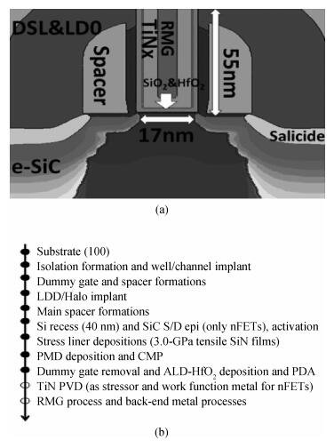
Fig. 1.
The cross sectional structures of (a) HK/MG nMOS and (b) process flow in simulation
SEMICONDUCTOR TECHNOLOGY
Zuozhen Fu, Huaxiang Yin, Xiaolong Ma, Shumin Chai, Jianfeng Gao and Dapeng Chen
Corresponding author: Fu Zuozhen, Email:fuzuozhen@ime.ac.cn; Yin Huaxiang, yinhuaxiang@ime.ac.cn
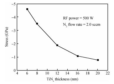
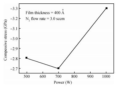
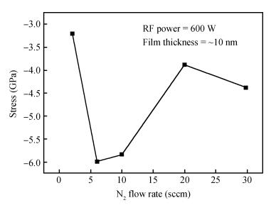
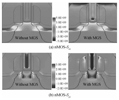
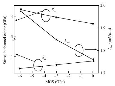
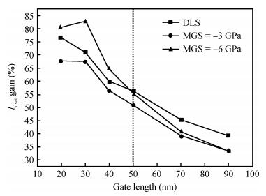
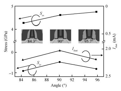
Abstract: The optimizations to metal gate structure and film process were extensively investigated for great metal-gate stress (MGS) in 20 nm high-k/metal-gate-last (HK/MG-last) nMOS devices. The characteristics of advanced MGS technologies on device performances were studied through a process and device simulation by TCAD tools. The metal gate electrode with different stress values (0 to-6 GPa) was implemented in the device simulation along with other traditional process-induced-strain (PIS) technologies like e-SiC and nitride capping layer. The MGS demonstrated a great enhancing effect on channel carriers transporting in the device as device pitch scaling down. In addition, the novel structure for a tilted gate electrode was proposed and relationships between the tilt angle and channel stress were investigated. Also with a new method of fully stressed replacement metal gate (FSRMG) and using plane-shape-HfO to substitute U-shape-HfO, the effect of MGS was improved. For greater film stress in the metal gate, the process conditions for physical vapor deposition (PVD) TiNx were optimized. The maximum compressive stress of-6.5 GPa TiNx was achieved with thinner film and greater RF power as well as about 6 sccm N ratio.
Keywords: metal gate stress, 20 nm CMOS devices, high-k/metal gate, PVD, TiNx
| [1] |
Tan K, Zhu M, Fang W, et al. A new liner stressor with very high intrinsic stree (>> 6 GPa) and low permittivity comprising diamond-like carbon (DLC) for strained p-channel transistors. IEEE International Electron Devices Meeting, 2007:127
|
| [2] |
Auth C, Cappellani A, Chun J S. 45 nm high-k + metal gate strain-enhanced transistors. Symposium on VLSI Technology, 2008:128 http://ieeexplore.ieee.org/document/4588589/
|
| [3] |
Hyun S, Han J, Park H. Aggressively scaled high-k last metal gate stack with low variability for 20 nm logic high performance and low power applications. Symposium on VLSI Technology (VLSIT), 2011:32 http://ieeexplore.ieee.org/document/5984618/
|
| [4] |
Chu M, Sun N, Thompson S E. A solution for higher carrier mobility in nanoscale MOSFETs. Annu Rev Mater Res, 2009, 39:203 doi: 10.1146/annurev-matsci-082908-145312
|
| [5] |
Sentaurus Device User Guide, Version D-2010. 03, Mountain View, California: Synopsys, Inc. , 2010
|
| [6] |
Kamminga J D, de Keijser T H, Delhez R. A model for stress in thin layers induced by misfitting particles:an origin for growth stress. Thin Solid Films, 1998, 317(1/2):169 http://adsabs.harvard.edu/abs/1998TSF...317..169K
|


Article views: 3385 Times PDF downloads: 54 Times Cited by: 0 Times
Received: 30 October 2012 Revised: 07 December 2012 Online: Published: 01 June 2013
| Citation: |
Zuozhen Fu, Huaxiang Yin, Xiaolong Ma, Shumin Chai, Jianfeng Gao, Dapeng Chen. Structure design and film process optimization for metal-gate stress in 20 nm nMOS devices[J]. Journal of Semiconductors, 2013, 34(6): 066002. doi: 10.1088/1674-4926/34/6/066002
****
Z Z Fu, H X Yin, X L Ma, S M Chai, J F Gao, D P Chen. Structure design and film process optimization for metal-gate stress in 20 nm nMOS devices[J]. J. Semicond., 2013, 34(6): 066002. doi: 10.1088/1674-4926/34/6/066002.

|
| [1] |
Tan K, Zhu M, Fang W, et al. A new liner stressor with very high intrinsic stree (>> 6 GPa) and low permittivity comprising diamond-like carbon (DLC) for strained p-channel transistors. IEEE International Electron Devices Meeting, 2007:127
|
| [2] |
Auth C, Cappellani A, Chun J S. 45 nm high-k + metal gate strain-enhanced transistors. Symposium on VLSI Technology, 2008:128 http://ieeexplore.ieee.org/document/4588589/
|
| [3] |
Hyun S, Han J, Park H. Aggressively scaled high-k last metal gate stack with low variability for 20 nm logic high performance and low power applications. Symposium on VLSI Technology (VLSIT), 2011:32 http://ieeexplore.ieee.org/document/5984618/
|
| [4] |
Chu M, Sun N, Thompson S E. A solution for higher carrier mobility in nanoscale MOSFETs. Annu Rev Mater Res, 2009, 39:203 doi: 10.1146/annurev-matsci-082908-145312
|
| [5] |
Sentaurus Device User Guide, Version D-2010. 03, Mountain View, California: Synopsys, Inc. , 2010
|
| [6] |
Kamminga J D, de Keijser T H, Delhez R. A model for stress in thin layers induced by misfitting particles:an origin for growth stress. Thin Solid Films, 1998, 317(1/2):169 http://adsabs.harvard.edu/abs/1998TSF...317..169K
|

 WeChat ID
Journal of Semiconductors © 2017 All Rights Reserved 京ICP备05085259号-2

 DownLoad: