


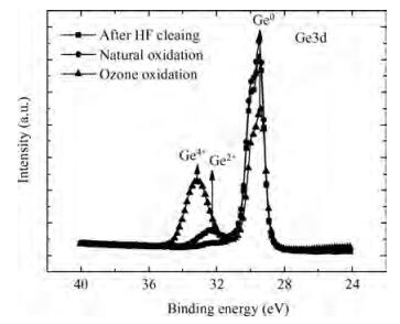
Fig. 1.
Ge3d spectra analyzed by XPS for wafers with different process conditions
SEMICONDUCTOR TECHNOLOGY
Mei Zhao, Renrong Liang, Jing Wang and Jun Xu
Corresponding author: Xu Jun, Email:junxu@tsinghua.edu.cn
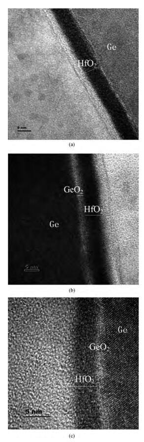
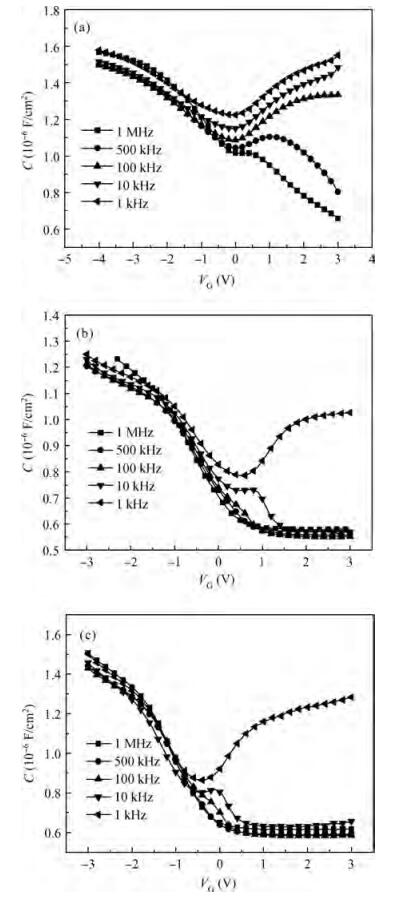
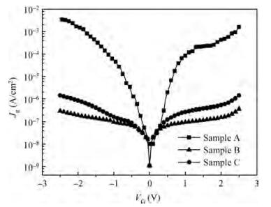
Abstract: The physical and electrical properties of a Ge/GeO2/HfO2/Al gate stack are investigated. A thin interfacial GeO2 layer (~1 nm) is formed between Ge and HfO2 by dual ozone treatments, which passivates the Ge/high-k interface. Capacitors on p-type Ge substrates show very promising capacitance-voltage (C-V) characteristics by using in situ pre-gate ozone passivation and ozone ambient annealing after high-k deposition, indicating efficient passivation of the Ge/HfO2 interface. It is shown that the mid-gap interface state density at the Ge/GeO2 interface is 6.4×1011 cm-2·eV-1. In addition, the gate leakage current density of the Ge/GeO2/HfO2/Al gate stack passivated by the dual ozone treatments is reduced by about three orders of magnitude compared to that of a Ge/HfO2/Al gate stack without interface passivation.
Keywords: germanium, surface passivation, ozone treatment, interface trap density, gate leakage current density
| [1] |
Kamata Y. High-k/Ge MOSFETs for future nanoelectronics. Mater Today, 2008, 11(1):30
|
| [2] |
Shang H, Frank M M, Gusev E P, et al. Germanium channel MOSFETs:opportunities and challenges. IBM J Res Develop, 2006, 50(4):377
|
| [3] |
Caymax M, Eneman G, Bellenger F, et al. Germanium for advanced CMOS anno 2009:a SWOT analysis. IEDM Tech Dig, 2009:461
|
| [4] |
Gusev E P, Shang H, Copel M, et al. Microstructure and thermal stability of HfO2 gate dielectric deposited on Ge(100). Appl Phys Lett, 2004, 85(12):2334 doi: 10.1063/1.1794849
|
| [5] |
Chui C O, Ramanathan S, Triplet B B, et al. Germanium MOS capacitors incorporating ultrathin high-k gate dielectric. IEEE Electron Device Lett, 2002, 23(8):473 doi: 10.1109/LED.2002.801319
|
| [6] |
Kuzum D, Krishnamohan T, Pethe A J, et al. Ge-interface engineering with ozone oxidation for low interface-state density. IEEE Electron Device Lett, 2008, 29(4):328 doi: 10.1109/LED.2008.918272
|
| [7] |
Maeda T, Morita Y, Takagi S. Impact of Ge nitride interfacial layers on performance of metal gate/high-k Ge-nMISFETs. VLSI Symp Tech Dig, 2010:213
|
| [8] |
Kim K H, Gordon R J, Ritenour A, et al. Atomic layer deposition of insulating nitride interfacial layers for germanium metal oxide semiconductor field effect transistors with high-k oxide/tungsten nitride gate stacks. Appl Phys Lett, 2007, 90(21):212104 doi: 10.1063/1.2741609
|
| [9] |
Bellenger F, De Jaeger B, Merckling C, et al. High FET performance for a future CMOS GeO2-based technology. IEEE Electron Device Lett, 2010, 31(5):402 doi: 10.1109/LED.2010.2044011
|
| [10] |
Lee C H, Nishimura T, Saido N, et al. Record-high electron mobility in Ge n-MOSFETs exceeding Si universality. IEDM Tech Dig, 2009:457
|
| [11] |
Delabie A, Bellenger F, Houssa M, et al. Effective electrical passivation of Ge(100) for high-k gate dielectric layers using germanium oxide. Appl Phys Lett, 2007, 91(8):082904 doi: 10.1063/1.2773759
|
| [12] |
Fukuda Y, Yazaki Y, Otani Y, et al. Low-temperature formation of high-quality GeO2 interlayer for high-k gate dielectrics/Ge by electron-cyclotron-resonance plasma techniques. IEEE Trans Electron Devices, 2010, 57(1):282 doi: 10.1109/TED.2009.2035030
|
| [13] |
Chui C O, Kim H, McIntyre P C, et al. Atomic layer deposition of high-k dielectric for germanium MOS applications-substrate surface preparation. IEEE Electron Device Lett, 2004, 25:274 doi: 10.1109/LED.2004.827285
|
| [14] |
Prabhakaran K, Ogino T. Oxidation of Ge (100) and Ge (111) surfaces:an UPS and XPS study. Surf Sci, 1995, 325:263 doi: 10.1016/0039-6028(94)00746-2
|
| [15] |
Hubbard K J, Schlom D G. Thermodynamic stability of binary oxides in contact with silicon. J Mater Res, 1996, 11:2757 doi: 10.1557/JMR.1996.0350
|
| [16] |
Moreau M, Munteanu D, Autran J L, et al. Investigation of capacitance-voltage characteristics in Ge/high-k MOS devices. J Non Cryst Solids, 2009, 355(18-21):1171 doi: 10.1016/j.jnoncrysol.2009.01.056
|
| [17] |
Hill W A and Coleman C C. A single-frequency approximation for interface-state density determination. Solid-State Electron, 1980, 23:987 doi: 10.1016/0038-1101(80)90064-7
|
| [18] |
Lee C H, Nishimura T, Nagashio K, et al. High-electron-mobility Ge/GeO2 n-MOSFETs with two-step oxidation. IEEE Trans Electron Devices, 2011, 58(5):1295 doi: 10.1109/TED.2011.2111373
|


Article views: 2633 Times PDF downloads: 30 Times Cited by: 0 Times
Received: 13 November 2012 Revised: 11 December 2012 Online: Published: 01 June 2013
| Citation: |
Mei Zhao, Renrong Liang, Jing Wang, Jun Xu. Effective interface passivation of a Ge/HfO2 gate stack using ozone pre-gate treatment and ozone ambient annealing[J]. Journal of Semiconductors, 2013, 34(6): 066005. doi: 10.1088/1674-4926/34/6/066005
****
M Zhao, R R Liang, J Wang, J Xu. Effective interface passivation of a Ge/HfO2 gate stack using ozone pre-gate treatment and ozone ambient annealing[J]. J. Semicond., 2013, 34(6): 066005. doi: 10.1088/1674-4926/34/6/066005.

|
| [1] |
Kamata Y. High-k/Ge MOSFETs for future nanoelectronics. Mater Today, 2008, 11(1):30
|
| [2] |
Shang H, Frank M M, Gusev E P, et al. Germanium channel MOSFETs:opportunities and challenges. IBM J Res Develop, 2006, 50(4):377
|
| [3] |
Caymax M, Eneman G, Bellenger F, et al. Germanium for advanced CMOS anno 2009:a SWOT analysis. IEDM Tech Dig, 2009:461
|
| [4] |
Gusev E P, Shang H, Copel M, et al. Microstructure and thermal stability of HfO2 gate dielectric deposited on Ge(100). Appl Phys Lett, 2004, 85(12):2334 doi: 10.1063/1.1794849
|
| [5] |
Chui C O, Ramanathan S, Triplet B B, et al. Germanium MOS capacitors incorporating ultrathin high-k gate dielectric. IEEE Electron Device Lett, 2002, 23(8):473 doi: 10.1109/LED.2002.801319
|
| [6] |
Kuzum D, Krishnamohan T, Pethe A J, et al. Ge-interface engineering with ozone oxidation for low interface-state density. IEEE Electron Device Lett, 2008, 29(4):328 doi: 10.1109/LED.2008.918272
|
| [7] |
Maeda T, Morita Y, Takagi S. Impact of Ge nitride interfacial layers on performance of metal gate/high-k Ge-nMISFETs. VLSI Symp Tech Dig, 2010:213
|
| [8] |
Kim K H, Gordon R J, Ritenour A, et al. Atomic layer deposition of insulating nitride interfacial layers for germanium metal oxide semiconductor field effect transistors with high-k oxide/tungsten nitride gate stacks. Appl Phys Lett, 2007, 90(21):212104 doi: 10.1063/1.2741609
|
| [9] |
Bellenger F, De Jaeger B, Merckling C, et al. High FET performance for a future CMOS GeO2-based technology. IEEE Electron Device Lett, 2010, 31(5):402 doi: 10.1109/LED.2010.2044011
|
| [10] |
Lee C H, Nishimura T, Saido N, et al. Record-high electron mobility in Ge n-MOSFETs exceeding Si universality. IEDM Tech Dig, 2009:457
|
| [11] |
Delabie A, Bellenger F, Houssa M, et al. Effective electrical passivation of Ge(100) for high-k gate dielectric layers using germanium oxide. Appl Phys Lett, 2007, 91(8):082904 doi: 10.1063/1.2773759
|
| [12] |
Fukuda Y, Yazaki Y, Otani Y, et al. Low-temperature formation of high-quality GeO2 interlayer for high-k gate dielectrics/Ge by electron-cyclotron-resonance plasma techniques. IEEE Trans Electron Devices, 2010, 57(1):282 doi: 10.1109/TED.2009.2035030
|
| [13] |
Chui C O, Kim H, McIntyre P C, et al. Atomic layer deposition of high-k dielectric for germanium MOS applications-substrate surface preparation. IEEE Electron Device Lett, 2004, 25:274 doi: 10.1109/LED.2004.827285
|
| [14] |
Prabhakaran K, Ogino T. Oxidation of Ge (100) and Ge (111) surfaces:an UPS and XPS study. Surf Sci, 1995, 325:263 doi: 10.1016/0039-6028(94)00746-2
|
| [15] |
Hubbard K J, Schlom D G. Thermodynamic stability of binary oxides in contact with silicon. J Mater Res, 1996, 11:2757 doi: 10.1557/JMR.1996.0350
|
| [16] |
Moreau M, Munteanu D, Autran J L, et al. Investigation of capacitance-voltage characteristics in Ge/high-k MOS devices. J Non Cryst Solids, 2009, 355(18-21):1171 doi: 10.1016/j.jnoncrysol.2009.01.056
|
| [17] |
Hill W A and Coleman C C. A single-frequency approximation for interface-state density determination. Solid-State Electron, 1980, 23:987 doi: 10.1016/0038-1101(80)90064-7
|
| [18] |
Lee C H, Nishimura T, Nagashio K, et al. High-electron-mobility Ge/GeO2 n-MOSFETs with two-step oxidation. IEEE Trans Electron Devices, 2011, 58(5):1295 doi: 10.1109/TED.2011.2111373
|

 WeChat ID
Journal of Semiconductors © 2017 All Rights Reserved 京ICP备05085259号-2

 DownLoad:

