


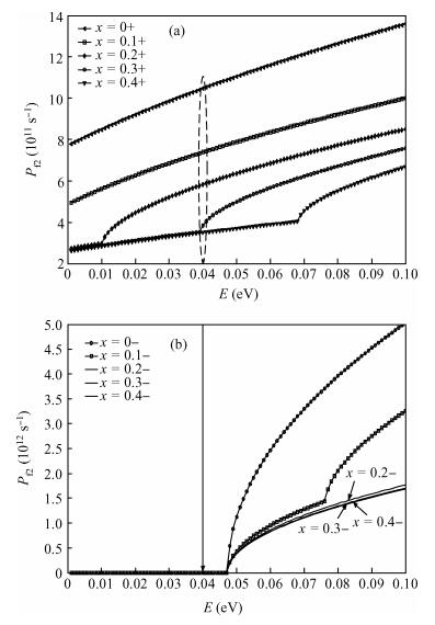
Fig. 1.
$P_{\rm f2}$ versus energy and Ge fraction at 300 K. (a) Absorption. (b) Emission
SEMICONDUCTOR PHYSICS
Zhao Jin1, , Liping Qiao2, Ce Liu1, Chen Guo1, Lidong Liu1 and Jiang'an Wang1
Corresponding author: Jin Zhao, Email:jinzhaogeorge@126.com
Abstract: Inter valley scattering has a great impact on carrier mobility of strained Si materials, so based on Fermi's golden rule and the theory of Boltzmann collision term approximation, inter valley phonon scattering mechanism of electrons in nano scale strained Si (101) materials is established under the influence of both energy and stress. It shows that inter valley phonon f2, f3, g3 scattering rates decrease markedly in nano scale strained Si (101) materials with increasing stress. The quantized models can provide valuable references to the understanding of strained Si materials and the research on electron carrier mobility.
Keywords: inter valley scattering, strained Si, model
| [1] |
Yang L F, Jeremy R W, Rechard C W, et al. Si/SiGe heterostructure parameters for device simulations. Semicond Sci Technol, 2004, 19(10):1174 doi: 10.1088/0268-1242/19/10/002
|
| [2] |
Song Jianjun, Zhang Heming, Hu Huiyong, et al. Determination of conduction band edge characteristics of strained Si/Si1-xGex. Chin Phys, 2007, 16(12):3827 doi: 10.1088/1009-1963/16/12/045
|
| [3] |
Zhao Lixia, Zhang Heming, Xuan Rongxi, et al. Scattering rates of electrons in strained Si1-xGex (100). Journal of Xidian University, 2012(3):86, 105
|
| [4] |
Liu H H, Duan X F, Xu Q X. Finite-element study of strain field in strained-Si MOSFET. Micron, 2009, 40:274 doi: 10.1016/j.micron.2008.06.005
|
| [5] |
Song Jianjun, Zhang Heming, Hu Huiyong, et al. Valence band structure of strained Si/(111) Si1-xGex. Science in China, Series G:Physics, Mechanics and Astronomy, 2010, 53(3):454 doi: 10.1007/s11433-010-0093-2
|
| [6] |
Olsen S H, Yan L, Aqaiby R, et al. Strained Si/SiGe MOS technology:improving gate dielectric integrity. Microelectron Eng, 2009, 86(3):218 doi: 10.1016/j.mee.2008.08.001
|
| [7] |
Smirnov S, Kosina H. Monte Carlo modeling of the electron mobility in strained Si1-xGex layers on arbitrarily oriented Si1-yGey substrates. Solid-State Electron, 2004, 48(8):1325 doi: 10.1016/j.sse.2004.01.014
|
| [8] |
Aubry F V, Dollfus P, Galdinn R S. Electron effective mobility in strained-Si/Si1-xGex MOS devices using Monte Carlo simulation. Solid-State Electron, 2005, 49(8):1320 doi: 10.1016/j.sse.2005.06.013
|
| [9] |
Driussi F, Esseni D, Selmi L, et al. On the electron mobility enhancement in biaxially strained Si MOSFETs. Solid-State Electron, 2008, 52(4):498 doi: 10.1016/j.sse.2007.10.033
|
| [10] |
Ye L X. Monte Carlo simulation for nano-scaled semiconductor devices. Beijing:Science Press, 1997:364
|
| [11] |
Song Jianjun, Zhang Heming, Shu Bin, et al. K.P dispersion relation near Δ_i valley in strained Si1-xGex/Si. Journal of Semiconductors, 2008, 29(3):442 http://www.jos.ac.cn/bdtxben/ch/reader/view_abstract.aspx?file_no=07042404&flag=1
|
| [12] |
Song Jianjun, Zhang Heming, Hu Huiyong, et al. Calculation of band structure in (101)-biaxially strained Si. Science in China, Series G:Physics, Mechanics and Astronomy, 2009, 52(4):546 doi: 10.1007/s11433-009-0078-1
|
| [13] |
Ye L X. Monte Carlo simulation for nano-scaled semiconductor devices. Beijing:Science Press, 1997:472
|
| [14] |
Wang Z C. Thermodynamics and statistical physics. 3rd ed. Beijing:National Defense Industry Press, 2003:263
|
| [15] |
Tang J Y, Hess K. Theory of hot electron emission from silicon into silicon dioxide. J Appl Phys, 1983, 54(9):5145 doi: 10.1063/1.332738
|
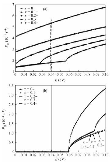
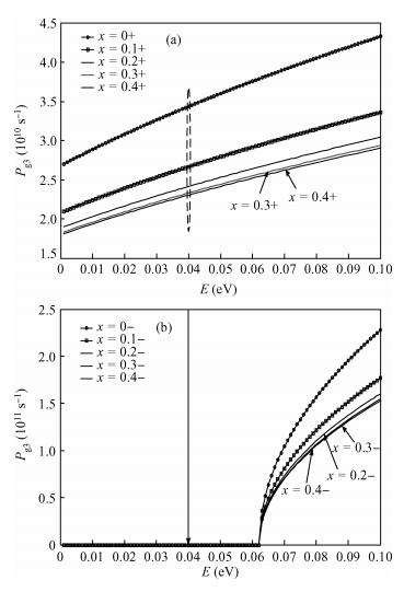
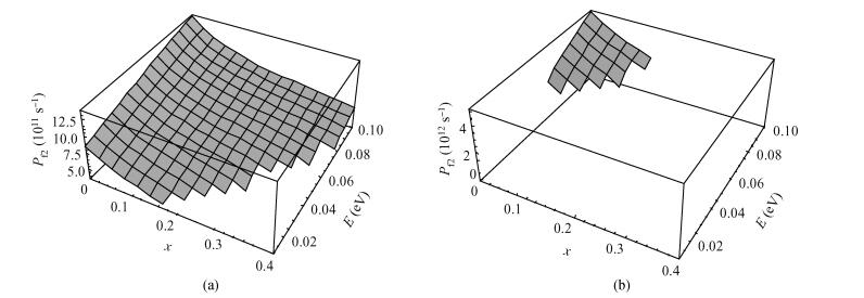
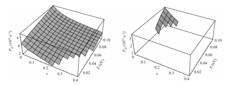

Table 1. Scattering parameters used in this paper

|
| [1] |
Yang L F, Jeremy R W, Rechard C W, et al. Si/SiGe heterostructure parameters for device simulations. Semicond Sci Technol, 2004, 19(10):1174 doi: 10.1088/0268-1242/19/10/002
|
| [2] |
Song Jianjun, Zhang Heming, Hu Huiyong, et al. Determination of conduction band edge characteristics of strained Si/Si1-xGex. Chin Phys, 2007, 16(12):3827 doi: 10.1088/1009-1963/16/12/045
|
| [3] |
Zhao Lixia, Zhang Heming, Xuan Rongxi, et al. Scattering rates of electrons in strained Si1-xGex (100). Journal of Xidian University, 2012(3):86, 105
|
| [4] |
Liu H H, Duan X F, Xu Q X. Finite-element study of strain field in strained-Si MOSFET. Micron, 2009, 40:274 doi: 10.1016/j.micron.2008.06.005
|
| [5] |
Song Jianjun, Zhang Heming, Hu Huiyong, et al. Valence band structure of strained Si/(111) Si1-xGex. Science in China, Series G:Physics, Mechanics and Astronomy, 2010, 53(3):454 doi: 10.1007/s11433-010-0093-2
|
| [6] |
Olsen S H, Yan L, Aqaiby R, et al. Strained Si/SiGe MOS technology:improving gate dielectric integrity. Microelectron Eng, 2009, 86(3):218 doi: 10.1016/j.mee.2008.08.001
|
| [7] |
Smirnov S, Kosina H. Monte Carlo modeling of the electron mobility in strained Si1-xGex layers on arbitrarily oriented Si1-yGey substrates. Solid-State Electron, 2004, 48(8):1325 doi: 10.1016/j.sse.2004.01.014
|
| [8] |
Aubry F V, Dollfus P, Galdinn R S. Electron effective mobility in strained-Si/Si1-xGex MOS devices using Monte Carlo simulation. Solid-State Electron, 2005, 49(8):1320 doi: 10.1016/j.sse.2005.06.013
|
| [9] |
Driussi F, Esseni D, Selmi L, et al. On the electron mobility enhancement in biaxially strained Si MOSFETs. Solid-State Electron, 2008, 52(4):498 doi: 10.1016/j.sse.2007.10.033
|
| [10] |
Ye L X. Monte Carlo simulation for nano-scaled semiconductor devices. Beijing:Science Press, 1997:364
|
| [11] |
Song Jianjun, Zhang Heming, Shu Bin, et al. K.P dispersion relation near Δ_i valley in strained Si1-xGex/Si. Journal of Semiconductors, 2008, 29(3):442 http://www.jos.ac.cn/bdtxben/ch/reader/view_abstract.aspx?file_no=07042404&flag=1
|
| [12] |
Song Jianjun, Zhang Heming, Hu Huiyong, et al. Calculation of band structure in (101)-biaxially strained Si. Science in China, Series G:Physics, Mechanics and Astronomy, 2009, 52(4):546 doi: 10.1007/s11433-009-0078-1
|
| [13] |
Ye L X. Monte Carlo simulation for nano-scaled semiconductor devices. Beijing:Science Press, 1997:472
|
| [14] |
Wang Z C. Thermodynamics and statistical physics. 3rd ed. Beijing:National Defense Industry Press, 2003:263
|
| [15] |
Tang J Y, Hess K. Theory of hot electron emission from silicon into silicon dioxide. J Appl Phys, 1983, 54(9):5145 doi: 10.1063/1.332738
|


Article views: 3890 Times PDF downloads: 14 Times Cited by: 0 Times
Received: 03 December 2012 Revised: 22 February 2013 Online: Published: 01 July 2013
| Citation: |
Zhao Jin, Liping Qiao, Ce Liu, Chen Guo, Lidong Liu, Jiang'an Wang. Inter valley phonon scattering mechanism in strained Si/(101) Si1-xGex[J]. Journal of Semiconductors, 2013, 34(7): 072002. doi: 10.1088/1674-4926/34/7/072002
****
Z Jin, L P Qiao, C Liu, C Guo, L D Liu, J A Wang. Inter valley phonon scattering mechanism in strained Si/(101) Si1-xGex[J]. J. Semicond., 2013, 34(7): 072002. doi: 10.1088/1674-4926/34/7/072002.

|
| [1] |
Yang L F, Jeremy R W, Rechard C W, et al. Si/SiGe heterostructure parameters for device simulations. Semicond Sci Technol, 2004, 19(10):1174 doi: 10.1088/0268-1242/19/10/002
|
| [2] |
Song Jianjun, Zhang Heming, Hu Huiyong, et al. Determination of conduction band edge characteristics of strained Si/Si1-xGex. Chin Phys, 2007, 16(12):3827 doi: 10.1088/1009-1963/16/12/045
|
| [3] |
Zhao Lixia, Zhang Heming, Xuan Rongxi, et al. Scattering rates of electrons in strained Si1-xGex (100). Journal of Xidian University, 2012(3):86, 105
|
| [4] |
Liu H H, Duan X F, Xu Q X. Finite-element study of strain field in strained-Si MOSFET. Micron, 2009, 40:274 doi: 10.1016/j.micron.2008.06.005
|
| [5] |
Song Jianjun, Zhang Heming, Hu Huiyong, et al. Valence band structure of strained Si/(111) Si1-xGex. Science in China, Series G:Physics, Mechanics and Astronomy, 2010, 53(3):454 doi: 10.1007/s11433-010-0093-2
|
| [6] |
Olsen S H, Yan L, Aqaiby R, et al. Strained Si/SiGe MOS technology:improving gate dielectric integrity. Microelectron Eng, 2009, 86(3):218 doi: 10.1016/j.mee.2008.08.001
|
| [7] |
Smirnov S, Kosina H. Monte Carlo modeling of the electron mobility in strained Si1-xGex layers on arbitrarily oriented Si1-yGey substrates. Solid-State Electron, 2004, 48(8):1325 doi: 10.1016/j.sse.2004.01.014
|
| [8] |
Aubry F V, Dollfus P, Galdinn R S. Electron effective mobility in strained-Si/Si1-xGex MOS devices using Monte Carlo simulation. Solid-State Electron, 2005, 49(8):1320 doi: 10.1016/j.sse.2005.06.013
|
| [9] |
Driussi F, Esseni D, Selmi L, et al. On the electron mobility enhancement in biaxially strained Si MOSFETs. Solid-State Electron, 2008, 52(4):498 doi: 10.1016/j.sse.2007.10.033
|
| [10] |
Ye L X. Monte Carlo simulation for nano-scaled semiconductor devices. Beijing:Science Press, 1997:364
|
| [11] |
Song Jianjun, Zhang Heming, Shu Bin, et al. K.P dispersion relation near Δ_i valley in strained Si1-xGex/Si. Journal of Semiconductors, 2008, 29(3):442 http://www.jos.ac.cn/bdtxben/ch/reader/view_abstract.aspx?file_no=07042404&flag=1
|
| [12] |
Song Jianjun, Zhang Heming, Hu Huiyong, et al. Calculation of band structure in (101)-biaxially strained Si. Science in China, Series G:Physics, Mechanics and Astronomy, 2009, 52(4):546 doi: 10.1007/s11433-009-0078-1
|
| [13] |
Ye L X. Monte Carlo simulation for nano-scaled semiconductor devices. Beijing:Science Press, 1997:472
|
| [14] |
Wang Z C. Thermodynamics and statistical physics. 3rd ed. Beijing:National Defense Industry Press, 2003:263
|
| [15] |
Tang J Y, Hess K. Theory of hot electron emission from silicon into silicon dioxide. J Appl Phys, 1983, 54(9):5145 doi: 10.1063/1.332738
|

 WeChat ID
Journal of Semiconductors © 2017 All Rights Reserved 京ICP备05085259号-2

 DownLoad:

