1. College of Electronic Engineering, Guangxi Normal University, Guilin 541004, ChinaCollege of Electronic Engineering, Guangxi Normal University, Guilin 541004, China
2. National Laboratory of Solid State Microstructures and Department of Physics, Nanjing University, Nanjing 210093, ChinaNational Laboratory of Solid State Microstructures and Department of Physics, Nanjing University, Nanjing 210093, China
3. Department of Physics, Chengde Teacher's College for Nationalities, Chengde 067000, ChinaDepartment of Physics, Chengde Teacher's College for Nationalities, Chengde 067000, China
Abstract: High pressure has a significant influence on β-FeSi2 band gaps and optical absorption tuning. In this work, using density functional theory, we investigate the effect of high pressure on the optical absorption behavior of a β-FeSi2 (100)/Si (001) interface with some Si vacancies. As the pressure increases, the optical absorption peak down-shifts firstly, reach minimum values, and then un-shifts slowly. The electronic orbital analysis indicates that the electronic transition between the highest occupied states and the lowest unoccupied states mainly originate from Fe atoms at the interface regions. Structural analysis discloses that the Si (001) slab partially offsets the pressure exerted on the β-FeSi2 (100) interface, but this effect will become weaker with further increasing pressure, and this physical mechanism plays an important role in its optical absorption behavior.
Because of its large optical absorption coefficient, a direct band gap (0.85 eV), abundance, and environmentally friendly element resources, semiconducting beta-phase iron disilicide (β-FeSi2) is useful for energy devices such as solar cells, photovoltaic devices, and thermoelectric devices[1-6]. A theoretical energy conversion efficiency of 16%-23% is predicted for β-FeSi2 solar cells[7, 8]. However, to date, there have been limited reports on solar cells fabricated using β-FeSi2, and the highest efficiency reported is 3.7% obtained on a crystalline β-FeSi2 film epitaxially grown on Si substrate[9]. However, this conversion efficiency is still too low to be practical because of the high reflectance from the β-FeSi2/Si interfacial layer. Therefore, the microstructure of the β-FeSi2/Si interface needs to be modified in order to enhance the photovoltaic performance. For example, to enhance trapping light efficiency, the traditional silicon substrates are replaced by textured ones to modify the interfacial structure. In addition, the photovoltaic characteristics can also be improved significantly by adding some Al atoms into the β-FeSi2/Si (100) interface regions[10]. Many reports imply that the β-FeSi2/Si interface is mainly responsible for the optical properties[11-15], but the intrinsic physical mechanism is not well clarified. As we all know, the optical absorption originates from the electronic transition between the conduction band (CB) and valence band (VB), therefore this becomes an important physical problem to clearly display the β-FeSi2/Si interface's electronic and optical absorption behavior.
Many calculations reveal that the optical absorption edge can be tuned by applied high pressure, especial for β-FeSi2 films structures. However, the effect of high pressure on the β-FeSi2/Si interface optical absorption behavior is rarely reported, due to its structure complexity. For example, when a β-FeSi2 film is deposited onto Si epitaxially, the diffusion rates of Fe and Si strongly depend on the preparation methods and, hence, the stoichiometry of the β-FeSi2/Si interface cannot be well controlled; some Si atoms are absent at the interfacial region, and this makes the lattice mismatch further increase[16, 17]. For β-FeSi2/Si interfacial structures, applied high pressure even effectively adjusts the lattice deformation extent systematically, and novel optical absorption behavior may occur. Therefore, a systematic investigation of the optical behavior and electronic structure of a β-FeSi2/Si interface with some Si vacancies at high pressure becomes an urgent objective. In this work, we theoretically display the behaviors of the optical absorption and electronic structures of the β-FeSi2/Si interface with some Si vacancies at different pressure.
2.
The model and calculation method
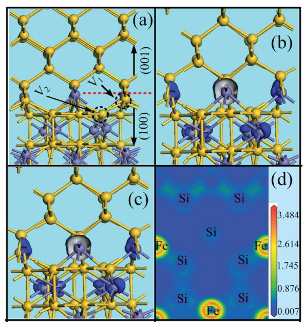
The heteroepitaxial system consisting of the β-FeSi2 (100)/Si (001) interfacial structure with some Si vacancies are simulated. The calculation is based on the density functional theory (DFT) in generalized gradient approximation (GGA) and Perdew-Burke-Ernzerhof (PBE) exchange-correlation potential, using the CASTEP package with Norm-conserving pseudopotentials[18, 19]. An energy cutoff of 500 eV is used to expand the plane wave functions. The Fe 3d64s2 orbitals and Si 3s23p2 orbitals are treated as valence states. The β-FeSi2 (100)/Si(001) interfacial layer is considered to comprise twelve layers of β-FeSi2 (100) and a Si (001) slabs, as shown in Fig. 1(a) and it has been verified to be well converged. The bottom two layers are fixed to mimic the bulk structure, and relaxation is performed until the following convergence tolerances are reached: 1 × 10⁻⁵ eV for energy, 0.03 eV/Å for maximum force, and 0.001 Å for maximum displacement. An external stress is applied by equivalent hydrostatic pressure and the optical properties are calculated based on the independent-particle approximation. The imaginary part of the dielectric function due to transitions between the occupied and unoccupied electronic states is given by the Fermi golden rule[20],
Figure
1.
(Color online) (a) Atomic configuration in the β-FeSi2 (100)/Si (001) model. The interfacial layer is marked by the red dashed line, the crystal orientations are marked by arrows, and gray and yellow balls represent Fe and Si atoms, respectively. The isosurfaces for electronic orbital of the highest occupied state and lowest unoccupied state of β-FeSi2 (100)/Si (001) interface with one Si atom absence at pressure P = 0 GPa are displayed in Figs. 1(b) and 1(c), respectively. The electronic density of the β-FeSi2 (100)/Si (001) interface with one Si atom absence is displayed in Fig. 1(d)
where Ω is the slab unit-cell volume, ℏω is the photon energy, k is the Bloch wave vector, Ec(v)k and |ψc(v)k(r)⟩ are the eigen-energy and wave function, where the superscripts c and v denote the states in the CB and the VB, respectively, r is the position vector, and u is the unit vector along the light polarization. We define the optical gaps as the energy at which the oscillator strength reaches 0.1% of the oscillator strength integrated from 0 to 1 eV. Although the DFT in the GGA is well known to underestimate band gaps, as our calculated band gap of 0.787 eV of bulk FeSi2 is much less than the experimental values of 0.875 eV, the trend of changing optical absorption behavior with applied pressure is reliable.
3.
Results and discussion
At pressure P = 0 GPa, the calculated photoabsorption and dielectric function imaginary part [Im ε] of the β-FeSi2 (100)/Si (001) interface structure containing different Si absences [positions V1 and V2, respectively marked by black circles in Fig. 1(a)] and without vacancies at are calculated and shown in Figs. 2(a) and 2(b), respectively. In the presence of Si vacancies (V1 and V2), the photoabsorption peaks are similar and without obvious difference, which imply that different Si vacancy positions at the interface layer cannot affect their optical behavior. Compared with the results of no vacancy, the Fe-Si bonds at the interface are enlarged form 3.429 to 3.463 Å, this leads to band gap and electronic structure changes[14]. Therefore, the up-shifts of photoabsorption peaks can be attributed to enlarged lattice distortion induced by Si vacancy addition. From the imaginary part of the dielectric function calculated results, we can obtain a similar physical phenomenon, which must be related with the internal electronic structure. Those results indicate that the existence of Si vacancies can affect the stress force imposed on the interface structure, but cannot directly affect the electronic transition between the CB and the VB, therefore the Fe atom state at the interfacial region is considered for this optical behavior.
Figure
2.
(a) Calculated photoabsorption spectra of the β-FeSi2 (100)/Si (001) interface with different Si vacancies at pressure $P =$ 0 GPa. (b) Calculated imaginary part of the dielectric function [Im ε] of the β-FeSi2 (100)/Si (001) interface with different Si vacancies at pressure $P =$ 0 GPa
To further confirm our conjectures, we examine the distribution of the electronic states at the VB and CB by orbital analysis. As pressure changes, the electronic orbital distributions are only slightly affected, but main features are very similar. As a typical characteristic, we display the electronic orbital analysis of the highest occupied states and lowest unoccupied states of the β-FeSi2 (100)/Si (001) interface with Si absence at pressure P = 2 GPa, in Figs. 1(b) and 1(c), respectively. This result obviously discloses that the electronic states are mainly dispersed in the regions of the interfacial Fe atom orbital, but slightly located at the internal Fe and Si atom orbital, which implies that the absence of some Si atoms in the interface cannot affect effectively the optical absorption and electronic transition. To further display electronic distribution behavior, the electronic density is also shown in Fig. 1(d), which also reveals that Fe atoms can tightly bind most electrons. After consideration about electronic structure, we can know that two β-FeSi2 atomic layers in the interfacial region should be mainly responsible for its optical absorption and dielectric function changes. Therefore, we can assume that the lattice distortion at interface as a result of a higher pressure can affect the optical behavior.
The photoabsorption spectra of β-FeSi2 (100)/Si (001) interface with Si vacancy (V1) at pressure P = 0, 1, 2, 3, 4 GPa are calculated and shown in Fig. 3(a). The calculated results show that the photoabsorption peak downshifts sharply to 0.26 eV from 0.21 eV with pressure increase to P = 2 GPa, and then begins to up-shift slowly to 0.35 eV for P = 4 GPa. From the definition of the imaginary part of the dielectric function, we can obtain the electronic transition feature between the lowest occupied and highest unoccupied electronic states. To clarify the photoabsorption physical origin, the imaginary parts of the dielectric function are also displayed in Fig. 3(b). Comparing to the results of photoabsorption, the similar changing features are displayed, which disclose that the lowest occupied and highest unoccupied electronic states are also affected by applied pressure; this may be a real physical reason for their optical behavior. From above analysis, the two interfacial layer atoms deformation as increasing pressure will be responsible for their optical behavior. Then we calculated the elastic constant (C44) for β-FeSi2 and Si, they are 127.1 GPa and 80.31 GPa, respectively. Therefore, the deformation difference as pressure increases will becomes obviously different, especially for interfacial regions with larger lattice mismatch[21]. So this physical process can be clearly displayed. As the pressure increases, the lengths of the Fe-Si bands at interfacial layers are decreased linearly form 2.297 Å (P = 0 GPa) to 2.288 Å (P = 1 GPa), 2.275 Å (P = 2 GPa), 2.273 Å (P = 3 GPa) and 2.269 Å (P = 4 GPa), and the lengths of the Fe-Si bands at internal region are also decreased linearly form 2.385 Å (P = 0 GPa) to 2.379 Å (P = 1 GPa), 2.375 Å (P = 2 GPa), 2.371 Å (P = 3 GPa) and 2.366 Å (P = 4 GPa). However, the difference in values between the interfacial and internal regions initially reaches a maximum 0.100 Å at P = 2 GPa and then decreases gradually to 0.097 Å at P = 4 GPa, which can partially offset the pressure exerted onto the β -FeSi2 (100) slab. This process will lead the absorption peak to down-shift firstly. As the pressure is further increased, the compressed Si (001) slab cannot offset effectively the applied pressure and consequently, the bond length difference decreases slowly. This special transformation in the interfacial region causes the electronic state distributions and electronic transition energy to change. And then the absorption peak slowly up-shifts. This explains why the β -FeSi2 (100)/Si (001) interface exhibits significantly different optical behavior and our study discloses that this phenomenon can be attributed to the deformation caused by different pressure. This behavior is obviously different from β-FeSi2 bulk materials. With increasing pressure, the optical gaps (Eg) of β -FeSi2 bulk materials are lineally enlarged: Eg = 0.78 eV (P = 0 GPa), 0.80 eV (P = 1 GPa), 0.81 eV (P = 2 GPa), 0.83 eV (P = 3 GPa), 0.85 eV (P = 4 GPa).
Figure
3.
(a) Calculated photoabsorption spectra of the β-FeSi2 (100)/Si (001) interface with a Si vacancy at pressure $P =$ 0, 1, 2, 3, 4 GPa. (b) Calculated imaginary part of the dielectric function [Im ε] of β-FeSi2 (100)/Si (001) interface with Si vacancy at pressure $P =$ 0, 1, 2, 3, 4 GPa
In summary, as pressure increases, the absorption spectra theoretically derived from the β-FeSi2 (100)/Si (001) slab indicate that the optical absorption peaks decrease initially, reach a minimum, and then increase gradually. Electronic structural analysis discloses that the Si (001) slab partially offsets the pressure exerted onto the β-FeSi2 (100) surface, and so the lengths of the Fe-Si and Si-Si bonds at the interface are larger than those in the internal region due to lattice mismatch itself, which is equivalent to strain applied to the interfacial region. As the pressure increases further, the compressed structure cannot offset effectively the high pressure, and then the absorption peak increases linearly with increasing pressure. This work discloses that pressure can play an important role in optical absorption behavior.
References
[1]
Noda K, Terai Y, Hasimoto S, et al. Modifications of direct transition energies in β-FeSi2 epitaxial films grown by molecular beam epitaxy. Appl Phys Lett, 2009, 94:241907 doi: 10.1063/1.3155204
[2]
Yamaguchi K, Mizushima K. Luminescent FeSi2 crystal structure induced by heteroepitaxial stress on Si (111). Phys Rev Lett, 2001, 86:6006 doi: 10.1103/PhysRevLett.86.6006
[3]
Leong D, Harry M, Reeson K J, et al. A silicon/iron-disilicide light-emitting diode operating at a wavelength of 1.5μm. Nature (London), 1997, 387:686 doi: 10.1038/42667
[4]
Tani J, Takahashi M, Kido H. Lattice dynamics of β-FeSi2 from first-principles calculations. Phys B, 2010, 405:2200 doi: 10.1016/j.physb.2010.02.008
[5]
Tassis D H, Mitsas C L, Zorba T T, et al. Infrared spectroscopic and electronic transport properties of polycrystalline semiconducting FeSi2 thin films. J Appl Phys, 1996, 80:962 doi: 10.1063/1.362908
[6]
Ito M, Nagai H, Oda E, et al. Effects of P doping on the thermoelectric properties of β-FeSi2. J Appl Phys, 2002, 91:2138 doi: 10.1063/1.1436302
[7]
Ootsuka T, Liu Z X, Osamura M, et al. Studies on aluminum-doped ZnO films for transparent electrode and antireflection coating of β-FeSi2 optoelectronic devices. Thin Solid Films, 2005, 476:30 doi: 10.1016/j.tsf.2004.06.145
[8]
Makita Y, Nakayama Y, Fukuzawa Y, et al. Important research targets to be explored for β-FeSi2 device making. Thin Solid Films, 2004, 461:202 doi: 10.1016/j.tsf.2004.02.073
[9]
Xu J X, Yao R H, Liu Y R. Growth of β-FeSi2 thin film on textured silicon substrate for solar cell application. Appl Surf Sci, 2011, 257:10168 doi: 10.1016/j.apsusc.2011.07.011
[10]
Dalapati G K, Liew S L, Wong A S W, et al. Photovoltaic characteristics of p-β-FeSi2(Al)/n-Si (100) heterojunction solar cells and the effects of interfacial engineering. Appl Phys Lett, 2011, 98:013507 doi: 10.1063/1.3536523
[11]
Leong D N, Harry M A, Resson K J, et al. On the origin of the 1.5μm luminescence in ion beam synthesized β-FeSi2. Appl Phys Lett, 1996, 68:1649 doi: 10.1063/1.115893
[12]
Takarabe K, Teranishi R, Oinuma J, et al. Optical properties of β-FeSi2 under pressure. Phys Rev B, 2002, 65:165215 doi: 10.1103/PhysRevB.65.165215
[13]
Clark S J, Al-Allak H M, Brand S, et al. Structure and electronic properties of FeSi2. Phys Rev B, 1998, 58:10389 doi: 10.1103/PhysRevB.58.10389
[14]
Miglio L, Meregalli V, Jepsen O. Strain dependent gap nature of epitaxial β-FeSi2 in silicon by first principles calculations. Appl Phys Lett, 1999, 75:385 doi: 10.1063/1.124383
[15]
Tani J I, Takahashi M, Kido H. First-principles calculations of the structure and elastic properties of β-FeSi2 at high-press. Intermetallics, 2010, 18:1222 doi: 10.1016/j.intermet.2010.03.023
[16]
Miki T, Matsui Y, Teraoka Y, et al. Point defects and thermoelectric properties of iron disilicide ceramics sintered with SiH4-plasma-processed micrograins. J Appl Phys, 1994, 76:2097 doi: 10.1063/1.357620
[17]
Liu Z X, Tanaka M, Kuroda R, et al. Influence of Si/Fe ratio in multilayer structures on crystalline growth of β-FeSi2 thin film on Si substrate. Appl Phys Lett, 2008, 93:021907 doi: 10.1063/1.2957990
[18]
Hamann D R, Schluter M, Chiang C. Norm-conserving pseudopotentials. Phys Rev Lett, 1979, 43:1494 doi: 10.1103/PhysRevLett.43.1494
[19]
Perdew J P, Burke K, Ernzerhof M. Generalized gradient approximation made simple. Phys Rev Lett, 1996, 77:3865 doi: 10.1103/PhysRevLett.77.3865
[20]
Liu L Z, W. Xu, Wu X L, et al. Electronic states and photoluminescence of TiO2 nanotubes with adsorbed surface oxygen. Appl Phys Lett, 2012, 100:121904 doi: 10.1063/1.3695167
[21]
Liu L Z, Wu X L, Liu X X, et al. Electronic structure and optical properties of β-FeSi2 (100)/Si (001) interface at high pressure. Appl Phys Lett, 2012, 101:111909 doi: 10.1063/1.4752154
Fig. 1.
(Color online) (a) Atomic configuration in the β-FeSi2 (100)/Si (001) model. The interfacial layer is marked by the red dashed line, the crystal orientations are marked by arrows, and gray and yellow balls represent Fe and Si atoms, respectively. The isosurfaces for electronic orbital of the highest occupied state and lowest unoccupied state of β-FeSi2 (100)/Si (001) interface with one Si atom absence at pressure P = 0 GPa are displayed in Figs. 1(b) and 1(c), respectively. The electronic density of the β-FeSi2 (100)/Si (001) interface with one Si atom absence is displayed in Fig. 1(d)
Fig. 2.
(a) Calculated photoabsorption spectra of the β-FeSi2 (100)/Si (001) interface with different Si vacancies at pressure $P =$ 0 GPa. (b) Calculated imaginary part of the dielectric function [Im ε] of the β-FeSi2 (100)/Si (001) interface with different Si vacancies at pressure $P =$ 0 GPa
Fig. 3.
(a) Calculated photoabsorption spectra of the β-FeSi2 (100)/Si (001) interface with a Si vacancy at pressure $P =$ 0, 1, 2, 3, 4 GPa. (b) Calculated imaginary part of the dielectric function [Im ε] of β-FeSi2 (100)/Si (001) interface with Si vacancy at pressure $P =$ 0, 1, 2, 3, 4 GPa
Noda K, Terai Y, Hasimoto S, et al. Modifications of direct transition energies in β-FeSi2 epitaxial films grown by molecular beam epitaxy. Appl Phys Lett, 2009, 94:241907 doi: 10.1063/1.3155204
[2]
Yamaguchi K, Mizushima K. Luminescent FeSi2 crystal structure induced by heteroepitaxial stress on Si (111). Phys Rev Lett, 2001, 86:6006 doi: 10.1103/PhysRevLett.86.6006
[3]
Leong D, Harry M, Reeson K J, et al. A silicon/iron-disilicide light-emitting diode operating at a wavelength of 1.5μm. Nature (London), 1997, 387:686 doi: 10.1038/42667
[4]
Tani J, Takahashi M, Kido H. Lattice dynamics of β-FeSi2 from first-principles calculations. Phys B, 2010, 405:2200 doi: 10.1016/j.physb.2010.02.008
[5]
Tassis D H, Mitsas C L, Zorba T T, et al. Infrared spectroscopic and electronic transport properties of polycrystalline semiconducting FeSi2 thin films. J Appl Phys, 1996, 80:962 doi: 10.1063/1.362908
[6]
Ito M, Nagai H, Oda E, et al. Effects of P doping on the thermoelectric properties of β-FeSi2. J Appl Phys, 2002, 91:2138 doi: 10.1063/1.1436302
[7]
Ootsuka T, Liu Z X, Osamura M, et al. Studies on aluminum-doped ZnO films for transparent electrode and antireflection coating of β-FeSi2 optoelectronic devices. Thin Solid Films, 2005, 476:30 doi: 10.1016/j.tsf.2004.06.145
[8]
Makita Y, Nakayama Y, Fukuzawa Y, et al. Important research targets to be explored for β-FeSi2 device making. Thin Solid Films, 2004, 461:202 doi: 10.1016/j.tsf.2004.02.073
[9]
Xu J X, Yao R H, Liu Y R. Growth of β-FeSi2 thin film on textured silicon substrate for solar cell application. Appl Surf Sci, 2011, 257:10168 doi: 10.1016/j.apsusc.2011.07.011
[10]
Dalapati G K, Liew S L, Wong A S W, et al. Photovoltaic characteristics of p-β-FeSi2(Al)/n-Si (100) heterojunction solar cells and the effects of interfacial engineering. Appl Phys Lett, 2011, 98:013507 doi: 10.1063/1.3536523
[11]
Leong D N, Harry M A, Resson K J, et al. On the origin of the 1.5μm luminescence in ion beam synthesized β-FeSi2. Appl Phys Lett, 1996, 68:1649 doi: 10.1063/1.115893
[12]
Takarabe K, Teranishi R, Oinuma J, et al. Optical properties of β-FeSi2 under pressure. Phys Rev B, 2002, 65:165215 doi: 10.1103/PhysRevB.65.165215
[13]
Clark S J, Al-Allak H M, Brand S, et al. Structure and electronic properties of FeSi2. Phys Rev B, 1998, 58:10389 doi: 10.1103/PhysRevB.58.10389
[14]
Miglio L, Meregalli V, Jepsen O. Strain dependent gap nature of epitaxial β-FeSi2 in silicon by first principles calculations. Appl Phys Lett, 1999, 75:385 doi: 10.1063/1.124383
[15]
Tani J I, Takahashi M, Kido H. First-principles calculations of the structure and elastic properties of β-FeSi2 at high-press. Intermetallics, 2010, 18:1222 doi: 10.1016/j.intermet.2010.03.023
[16]
Miki T, Matsui Y, Teraoka Y, et al. Point defects and thermoelectric properties of iron disilicide ceramics sintered with SiH4-plasma-processed micrograins. J Appl Phys, 1994, 76:2097 doi: 10.1063/1.357620
[17]
Liu Z X, Tanaka M, Kuroda R, et al. Influence of Si/Fe ratio in multilayer structures on crystalline growth of β-FeSi2 thin film on Si substrate. Appl Phys Lett, 2008, 93:021907 doi: 10.1063/1.2957990
[18]
Hamann D R, Schluter M, Chiang C. Norm-conserving pseudopotentials. Phys Rev Lett, 1979, 43:1494 doi: 10.1103/PhysRevLett.43.1494
[19]
Perdew J P, Burke K, Ernzerhof M. Generalized gradient approximation made simple. Phys Rev Lett, 1996, 77:3865 doi: 10.1103/PhysRevLett.77.3865
[20]
Liu L Z, W. Xu, Wu X L, et al. Electronic states and photoluminescence of TiO2 nanotubes with adsorbed surface oxygen. Appl Phys Lett, 2012, 100:121904 doi: 10.1063/1.3695167
[21]
Liu L Z, Wu X L, Liu X X, et al. Electronic structure and optical properties of β-FeSi2 (100)/Si (001) interface at high pressure. Appl Phys Lett, 2012, 101:111909 doi: 10.1063/1.4752154
Lin Yuanhua, Wang Jianfei, He Hongcai, Zhou Jianping, Zhou Xisong, et al.
Chinese Journal of Semiconductors , 2005, 26(S1): 74-77.
Search
GET CITATION
Haitao Li, Jun Qian, Fangfang Han, Tinghui Li. Density functional theory studies of the optical properties of a β-FeSi2 (100)/Si (001) interface at high pressure[J]. Journal of Semiconductors, 2013, 34(7): 072003. doi: 10.1088/1674-4926/34/7/072003
H T Li, J Qian, F F Han, T H Li. Density functional theory studies of the optical properties of a β-FeSi2 (100)/Si (001) interface at high pressure[J]. J. Semicond., 2013, 34(7): 072003. doi: 10.1088/1674-4926/34/7/072003.
Export: BibTexEndNote
Share:
Article Metrics
Article views: 2309 TimesPDF downloads: 13 TimesCited by: 0 Times
History
Received: 06 November 2012Revised: 23 January 2013Online:Published: 01 July 2013
Haitao Li, Jun Qian, Fangfang Han, Tinghui Li. Density functional theory studies of the optical properties of a β-FeSi2 (100)/Si (001) interface at high pressure[J]. Journal of Semiconductors, 2013, 34(7): 072003. doi: 10.1088/1674-4926/34/7/072003 ****H T Li, J Qian, F F Han, T H Li. Density functional theory studies of the optical properties of a β-FeSi2 (100)/Si (001) interface at high pressure[J]. J. Semicond., 2013, 34(7): 072003. doi: 10.1088/1674-4926/34/7/072003.
Citation:
Haitao Li, Jun Qian, Fangfang Han, Tinghui Li. Density functional theory studies of the optical properties of a β-FeSi2 (100)/Si (001) interface at high pressure[J]. Journal of Semiconductors, 2013, 34(7): 072003. doi: 10.1088/1674-4926/34/7/072003
****
H T Li, J Qian, F F Han, T H Li. Density functional theory studies of the optical properties of a β-FeSi2 (100)/Si (001) interface at high pressure[J]. J. Semicond., 2013, 34(7): 072003. doi: 10.1088/1674-4926/34/7/072003.
High pressure has a significant influence on β-FeSi2 band gaps and optical absorption tuning. In this work, using density functional theory, we investigate the effect of high pressure on the optical absorption behavior of a β-FeSi2 (100)/Si (001) interface with some Si vacancies. As the pressure increases, the optical absorption peak down-shifts firstly, reach minimum values, and then un-shifts slowly. The electronic orbital analysis indicates that the electronic transition between the highest occupied states and the lowest unoccupied states mainly originate from Fe atoms at the interface regions. Structural analysis discloses that the Si (001) slab partially offsets the pressure exerted on the β-FeSi2 (100) interface, but this effect will become weaker with further increasing pressure, and this physical mechanism plays an important role in its optical absorption behavior.
Because of its large optical absorption coefficient, a direct band gap (0.85 eV), abundance, and environmentally friendly element resources, semiconducting beta-phase iron disilicide (β-FeSi2) is useful for energy devices such as solar cells, photovoltaic devices, and thermoelectric devices[1-6]. A theoretical energy conversion efficiency of 16%-23% is predicted for β-FeSi2 solar cells[7, 8]. However, to date, there have been limited reports on solar cells fabricated using β-FeSi2, and the highest efficiency reported is 3.7% obtained on a crystalline β-FeSi2 film epitaxially grown on Si substrate[9]. However, this conversion efficiency is still too low to be practical because of the high reflectance from the β-FeSi2/Si interfacial layer. Therefore, the microstructure of the β-FeSi2/Si interface needs to be modified in order to enhance the photovoltaic performance. For example, to enhance trapping light efficiency, the traditional silicon substrates are replaced by textured ones to modify the interfacial structure. In addition, the photovoltaic characteristics can also be improved significantly by adding some Al atoms into the β-FeSi2/Si (100) interface regions[10]. Many reports imply that the β-FeSi2/Si interface is mainly responsible for the optical properties[11-15], but the intrinsic physical mechanism is not well clarified. As we all know, the optical absorption originates from the electronic transition between the conduction band (CB) and valence band (VB), therefore this becomes an important physical problem to clearly display the β-FeSi2/Si interface's electronic and optical absorption behavior.
Many calculations reveal that the optical absorption edge can be tuned by applied high pressure, especial for β-FeSi2 films structures. However, the effect of high pressure on the β-FeSi2/Si interface optical absorption behavior is rarely reported, due to its structure complexity. For example, when a β-FeSi2 film is deposited onto Si epitaxially, the diffusion rates of Fe and Si strongly depend on the preparation methods and, hence, the stoichiometry of the β-FeSi2/Si interface cannot be well controlled; some Si atoms are absent at the interfacial region, and this makes the lattice mismatch further increase[16, 17]. For β-FeSi2/Si interfacial structures, applied high pressure even effectively adjusts the lattice deformation extent systematically, and novel optical absorption behavior may occur. Therefore, a systematic investigation of the optical behavior and electronic structure of a β-FeSi2/Si interface with some Si vacancies at high pressure becomes an urgent objective. In this work, we theoretically display the behaviors of the optical absorption and electronic structures of the β-FeSi2/Si interface with some Si vacancies at different pressure.
2.
The model and calculation method
The heteroepitaxial system consisting of the β-FeSi2 (100)/Si (001) interfacial structure with some Si vacancies are simulated. The calculation is based on the density functional theory (DFT) in generalized gradient approximation (GGA) and Perdew-Burke-Ernzerhof (PBE) exchange-correlation potential, using the CASTEP package with Norm-conserving pseudopotentials[18, 19]. An energy cutoff of 500 eV is used to expand the plane wave functions. The Fe 3d64s2 orbitals and Si 3s23p2 orbitals are treated as valence states. The β-FeSi2 (100)/Si(001) interfacial layer is considered to comprise twelve layers of β-FeSi2 (100) and a Si (001) slabs, as shown in Fig. 1(a) and it has been verified to be well converged. The bottom two layers are fixed to mimic the bulk structure, and relaxation is performed until the following convergence tolerances are reached: 1 × 10⁻⁵ eV for energy, 0.03 eV/Å for maximum force, and 0.001 Å for maximum displacement. An external stress is applied by equivalent hydrostatic pressure and the optical properties are calculated based on the independent-particle approximation. The imaginary part of the dielectric function due to transitions between the occupied and unoccupied electronic states is given by the Fermi golden rule[20],
Figure
1.
(Color online) (a) Atomic configuration in the β-FeSi2 (100)/Si (001) model. The interfacial layer is marked by the red dashed line, the crystal orientations are marked by arrows, and gray and yellow balls represent Fe and Si atoms, respectively. The isosurfaces for electronic orbital of the highest occupied state and lowest unoccupied state of β-FeSi2 (100)/Si (001) interface with one Si atom absence at pressure P = 0 GPa are displayed in Figs. 1(b) and 1(c), respectively. The electronic density of the β-FeSi2 (100)/Si (001) interface with one Si atom absence is displayed in Fig. 1(d)
where Ω is the slab unit-cell volume, ℏω is the photon energy, k is the Bloch wave vector, Ec(v)k and |ψc(v)k(r)⟩ are the eigen-energy and wave function, where the superscripts c and v denote the states in the CB and the VB, respectively, r is the position vector, and u is the unit vector along the light polarization. We define the optical gaps as the energy at which the oscillator strength reaches 0.1% of the oscillator strength integrated from 0 to 1 eV. Although the DFT in the GGA is well known to underestimate band gaps, as our calculated band gap of 0.787 eV of bulk FeSi2 is much less than the experimental values of 0.875 eV, the trend of changing optical absorption behavior with applied pressure is reliable.
3.
Results and discussion
At pressure P = 0 GPa, the calculated photoabsorption and dielectric function imaginary part [Im ε] of the β-FeSi2 (100)/Si (001) interface structure containing different Si absences [positions V1 and V2, respectively marked by black circles in Fig. 1(a)] and without vacancies at are calculated and shown in Figs. 2(a) and 2(b), respectively. In the presence of Si vacancies (V1 and V2), the photoabsorption peaks are similar and without obvious difference, which imply that different Si vacancy positions at the interface layer cannot affect their optical behavior. Compared with the results of no vacancy, the Fe-Si bonds at the interface are enlarged form 3.429 to 3.463 Å, this leads to band gap and electronic structure changes[14]. Therefore, the up-shifts of photoabsorption peaks can be attributed to enlarged lattice distortion induced by Si vacancy addition. From the imaginary part of the dielectric function calculated results, we can obtain a similar physical phenomenon, which must be related with the internal electronic structure. Those results indicate that the existence of Si vacancies can affect the stress force imposed on the interface structure, but cannot directly affect the electronic transition between the CB and the VB, therefore the Fe atom state at the interfacial region is considered for this optical behavior.
Figure
2.
(a) Calculated photoabsorption spectra of the β-FeSi2 (100)/Si (001) interface with different Si vacancies at pressure $P =$ 0 GPa. (b) Calculated imaginary part of the dielectric function [Im ε] of the β-FeSi2 (100)/Si (001) interface with different Si vacancies at pressure $P =$ 0 GPa
To further confirm our conjectures, we examine the distribution of the electronic states at the VB and CB by orbital analysis. As pressure changes, the electronic orbital distributions are only slightly affected, but main features are very similar. As a typical characteristic, we display the electronic orbital analysis of the highest occupied states and lowest unoccupied states of the β-FeSi2 (100)/Si (001) interface with Si absence at pressure P = 2 GPa, in Figs. 1(b) and 1(c), respectively. This result obviously discloses that the electronic states are mainly dispersed in the regions of the interfacial Fe atom orbital, but slightly located at the internal Fe and Si atom orbital, which implies that the absence of some Si atoms in the interface cannot affect effectively the optical absorption and electronic transition. To further display electronic distribution behavior, the electronic density is also shown in Fig. 1(d), which also reveals that Fe atoms can tightly bind most electrons. After consideration about electronic structure, we can know that two β-FeSi2 atomic layers in the interfacial region should be mainly responsible for its optical absorption and dielectric function changes. Therefore, we can assume that the lattice distortion at interface as a result of a higher pressure can affect the optical behavior.
The photoabsorption spectra of β-FeSi2 (100)/Si (001) interface with Si vacancy (V1) at pressure P = 0, 1, 2, 3, 4 GPa are calculated and shown in Fig. 3(a). The calculated results show that the photoabsorption peak downshifts sharply to 0.26 eV from 0.21 eV with pressure increase to P = 2 GPa, and then begins to up-shift slowly to 0.35 eV for P = 4 GPa. From the definition of the imaginary part of the dielectric function, we can obtain the electronic transition feature between the lowest occupied and highest unoccupied electronic states. To clarify the photoabsorption physical origin, the imaginary parts of the dielectric function are also displayed in Fig. 3(b). Comparing to the results of photoabsorption, the similar changing features are displayed, which disclose that the lowest occupied and highest unoccupied electronic states are also affected by applied pressure; this may be a real physical reason for their optical behavior. From above analysis, the two interfacial layer atoms deformation as increasing pressure will be responsible for their optical behavior. Then we calculated the elastic constant (C44) for β-FeSi2 and Si, they are 127.1 GPa and 80.31 GPa, respectively. Therefore, the deformation difference as pressure increases will becomes obviously different, especially for interfacial regions with larger lattice mismatch[21]. So this physical process can be clearly displayed. As the pressure increases, the lengths of the Fe-Si bands at interfacial layers are decreased linearly form 2.297 Å (P = 0 GPa) to 2.288 Å (P = 1 GPa), 2.275 Å (P = 2 GPa), 2.273 Å (P = 3 GPa) and 2.269 Å (P = 4 GPa), and the lengths of the Fe-Si bands at internal region are also decreased linearly form 2.385 Å (P = 0 GPa) to 2.379 Å (P = 1 GPa), 2.375 Å (P = 2 GPa), 2.371 Å (P = 3 GPa) and 2.366 Å (P = 4 GPa). However, the difference in values between the interfacial and internal regions initially reaches a maximum 0.100 Å at P = 2 GPa and then decreases gradually to 0.097 Å at P = 4 GPa, which can partially offset the pressure exerted onto the β -FeSi2 (100) slab. This process will lead the absorption peak to down-shift firstly. As the pressure is further increased, the compressed Si (001) slab cannot offset effectively the applied pressure and consequently, the bond length difference decreases slowly. This special transformation in the interfacial region causes the electronic state distributions and electronic transition energy to change. And then the absorption peak slowly up-shifts. This explains why the β -FeSi2 (100)/Si (001) interface exhibits significantly different optical behavior and our study discloses that this phenomenon can be attributed to the deformation caused by different pressure. This behavior is obviously different from β-FeSi2 bulk materials. With increasing pressure, the optical gaps (Eg) of β -FeSi2 bulk materials are lineally enlarged: Eg = 0.78 eV (P = 0 GPa), 0.80 eV (P = 1 GPa), 0.81 eV (P = 2 GPa), 0.83 eV (P = 3 GPa), 0.85 eV (P = 4 GPa).
Figure
3.
(a) Calculated photoabsorption spectra of the β-FeSi2 (100)/Si (001) interface with a Si vacancy at pressure $P =$ 0, 1, 2, 3, 4 GPa. (b) Calculated imaginary part of the dielectric function [Im ε] of β-FeSi2 (100)/Si (001) interface with Si vacancy at pressure $P =$ 0, 1, 2, 3, 4 GPa
In summary, as pressure increases, the absorption spectra theoretically derived from the β-FeSi2 (100)/Si (001) slab indicate that the optical absorption peaks decrease initially, reach a minimum, and then increase gradually. Electronic structural analysis discloses that the Si (001) slab partially offsets the pressure exerted onto the β-FeSi2 (100) surface, and so the lengths of the Fe-Si and Si-Si bonds at the interface are larger than those in the internal region due to lattice mismatch itself, which is equivalent to strain applied to the interfacial region. As the pressure increases further, the compressed structure cannot offset effectively the high pressure, and then the absorption peak increases linearly with increasing pressure. This work discloses that pressure can play an important role in optical absorption behavior.
Noda K, Terai Y, Hasimoto S, et al. Modifications of direct transition energies in β-FeSi2 epitaxial films grown by molecular beam epitaxy. Appl Phys Lett, 2009, 94:241907 doi: 10.1063/1.3155204
[2]
Yamaguchi K, Mizushima K. Luminescent FeSi2 crystal structure induced by heteroepitaxial stress on Si (111). Phys Rev Lett, 2001, 86:6006 doi: 10.1103/PhysRevLett.86.6006
[3]
Leong D, Harry M, Reeson K J, et al. A silicon/iron-disilicide light-emitting diode operating at a wavelength of 1.5μm. Nature (London), 1997, 387:686 doi: 10.1038/42667
[4]
Tani J, Takahashi M, Kido H. Lattice dynamics of β-FeSi2 from first-principles calculations. Phys B, 2010, 405:2200 doi: 10.1016/j.physb.2010.02.008
[5]
Tassis D H, Mitsas C L, Zorba T T, et al. Infrared spectroscopic and electronic transport properties of polycrystalline semiconducting FeSi2 thin films. J Appl Phys, 1996, 80:962 doi: 10.1063/1.362908
[6]
Ito M, Nagai H, Oda E, et al. Effects of P doping on the thermoelectric properties of β-FeSi2. J Appl Phys, 2002, 91:2138 doi: 10.1063/1.1436302
[7]
Ootsuka T, Liu Z X, Osamura M, et al. Studies on aluminum-doped ZnO films for transparent electrode and antireflection coating of β-FeSi2 optoelectronic devices. Thin Solid Films, 2005, 476:30 doi: 10.1016/j.tsf.2004.06.145
[8]
Makita Y, Nakayama Y, Fukuzawa Y, et al. Important research targets to be explored for β-FeSi2 device making. Thin Solid Films, 2004, 461:202 doi: 10.1016/j.tsf.2004.02.073
[9]
Xu J X, Yao R H, Liu Y R. Growth of β-FeSi2 thin film on textured silicon substrate for solar cell application. Appl Surf Sci, 2011, 257:10168 doi: 10.1016/j.apsusc.2011.07.011
[10]
Dalapati G K, Liew S L, Wong A S W, et al. Photovoltaic characteristics of p-β-FeSi2(Al)/n-Si (100) heterojunction solar cells and the effects of interfacial engineering. Appl Phys Lett, 2011, 98:013507 doi: 10.1063/1.3536523
[11]
Leong D N, Harry M A, Resson K J, et al. On the origin of the 1.5μm luminescence in ion beam synthesized β-FeSi2. Appl Phys Lett, 1996, 68:1649 doi: 10.1063/1.115893
[12]
Takarabe K, Teranishi R, Oinuma J, et al. Optical properties of β-FeSi2 under pressure. Phys Rev B, 2002, 65:165215 doi: 10.1103/PhysRevB.65.165215
[13]
Clark S J, Al-Allak H M, Brand S, et al. Structure and electronic properties of FeSi2. Phys Rev B, 1998, 58:10389 doi: 10.1103/PhysRevB.58.10389
[14]
Miglio L, Meregalli V, Jepsen O. Strain dependent gap nature of epitaxial β-FeSi2 in silicon by first principles calculations. Appl Phys Lett, 1999, 75:385 doi: 10.1063/1.124383
[15]
Tani J I, Takahashi M, Kido H. First-principles calculations of the structure and elastic properties of β-FeSi2 at high-press. Intermetallics, 2010, 18:1222 doi: 10.1016/j.intermet.2010.03.023
[16]
Miki T, Matsui Y, Teraoka Y, et al. Point defects and thermoelectric properties of iron disilicide ceramics sintered with SiH4-plasma-processed micrograins. J Appl Phys, 1994, 76:2097 doi: 10.1063/1.357620
[17]
Liu Z X, Tanaka M, Kuroda R, et al. Influence of Si/Fe ratio in multilayer structures on crystalline growth of β-FeSi2 thin film on Si substrate. Appl Phys Lett, 2008, 93:021907 doi: 10.1063/1.2957990
[18]
Hamann D R, Schluter M, Chiang C. Norm-conserving pseudopotentials. Phys Rev Lett, 1979, 43:1494 doi: 10.1103/PhysRevLett.43.1494
[19]
Perdew J P, Burke K, Ernzerhof M. Generalized gradient approximation made simple. Phys Rev Lett, 1996, 77:3865 doi: 10.1103/PhysRevLett.77.3865
[20]
Liu L Z, W. Xu, Wu X L, et al. Electronic states and photoluminescence of TiO2 nanotubes with adsorbed surface oxygen. Appl Phys Lett, 2012, 100:121904 doi: 10.1063/1.3695167
[21]
Liu L Z, Wu X L, Liu X X, et al. Electronic structure and optical properties of β-FeSi2 (100)/Si (001) interface at high pressure. Appl Phys Lett, 2012, 101:111909 doi: 10.1063/1.4752154
Haitao Li, Jun Qian, Fangfang Han, Tinghui Li. Density functional theory studies of the optical properties of a β-FeSi2 (100)/Si (001) interface at high pressure[J]. Journal of Semiconductors, 2013, 34(7): 072003. doi: 10.1088/1674-4926/34/7/072003 ****H T Li, J Qian, F F Han, T H Li. Density functional theory studies of the optical properties of a β-FeSi2 (100)/Si (001) interface at high pressure[J]. J. Semicond., 2013, 34(7): 072003. doi: 10.1088/1674-4926/34/7/072003.
Haitao Li, Jun Qian, Fangfang Han, Tinghui Li. Density functional theory studies of the optical properties of a β-FeSi2 (100)/Si (001) interface at high pressure[J]. Journal of Semiconductors, 2013, 34(7): 072003. doi: 10.1088/1674-4926/34/7/072003
****
H T Li, J Qian, F F Han, T H Li. Density functional theory studies of the optical properties of a β-FeSi2 (100)/Si (001) interface at high pressure[J]. J. Semicond., 2013, 34(7): 072003. doi: 10.1088/1674-4926/34/7/072003.
Figure Fig. 1. (Color online) (a) Atomic configuration in the β-FeSi2 (100)/Si (001) model. The interfacial layer is marked by the red dashed line, the crystal orientations are marked by arrows, and gray and yellow balls represent Fe and Si atoms, respectively. The isosurfaces for electronic orbital of the highest occupied state and lowest unoccupied state of β-FeSi2 (100)/Si (001) interface with one Si atom absence at pressure P = 0 GPa are displayed in Figs. 1(b) and 1(c), respectively. The electronic density of the β-FeSi2 (100)/Si (001) interface with one Si atom absence is displayed in Fig. 1(d)
Figure Fig. 2. (a) Calculated photoabsorption spectra of the β-FeSi2 (100)/Si (001) interface with different Si vacancies at pressure $P =$ 0 GPa. (b) Calculated imaginary part of the dielectric function [Im ε] of the β-FeSi2 (100)/Si (001) interface with different Si vacancies at pressure $P =$ 0 GPa
Figure Fig. 3. (a) Calculated photoabsorption spectra of the β-FeSi2 (100)/Si (001) interface with a Si vacancy at pressure $P =$ 0, 1, 2, 3, 4 GPa. (b) Calculated imaginary part of the dielectric function [Im ε] of β-FeSi2 (100)/Si (001) interface with Si vacancy at pressure $P =$ 0, 1, 2, 3, 4 GPa