


Fig. 1.
Schematic diagrams of the approximation for (a) the infinite triangle-shaped confined potential, and (b) the square quantum well
SEMICONDUCTOR PHYSICS
Xiao Jin1, , Hong Zhang1, Rongxiu Zhou1 and Zhao Jin2
Corresponding author: Jin Xiao, Email:jinxiao0535@126.com
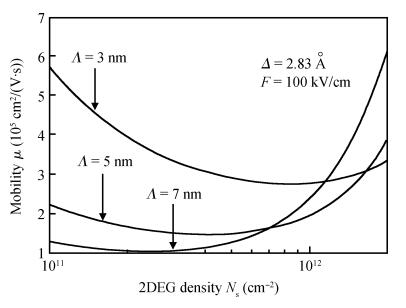
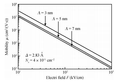
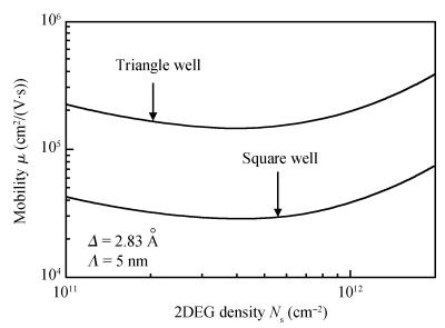
Abstract: We have theoretically studied the mobility limited by interface roughness scattering on two-dimensional electrons gas (2DEG) at a single heterointerface (triangle-shaped quantum well). Our results indicate that, like the interface roughness scattering in a square quantum well, the roughness scattering at the AlxGa1-xAs/GaAs heterointerface can be characterized by parameters of roughness height Δ and lateral Λ, and in addition by electric field F. A comparison of two mobilities limited by the interface roughness scattering between the present result and a square well in the same condition is given.
Keywords: mobility, AlGaAs/GaAs, interface roughness scattering
| [1] |
Dutta G, Basu S. Analysis of the electrical characteristics of GaInP/GaAs HBTs including the recombination effect. Journal of Semiconductors, 2012, 33(5):054002 doi: 10.1088/1674-4926/33/5/054002
|
| [2] |
Gold A. Electronic transport properties of a two-dimensional electron gas in a silicon quantum-well structure at low temperature. Phys Rev B, 1987, 35:723 doi: 10.1103/PhysRevB.35.723
|
| [3] |
Sakaki H, Noda T, Hirakawa K, et al. Interface roughness scattering in GaAs/AlAs quantum wells. Appl Phys Lett, 1987, 51:1934 doi: 10.1063/1.98305
|
| [4] |
Joshi R P. Simulations for the high-speed response of GaN metal-semiconductor-metal photodetectors. Appl Phys Lett, 1994, 64:223 doi: 10.1063/1.111511
|
| [5] |
Mou C Y, Hong T M. Transport in quantum wells in the presence of interface roughness. Phys Rev B, 2000, 61:12612 doi: 10.1103/PhysRevB.61.12612
|
| [6] |
Li Ran, Huang Hui, Ren Xiaomin, et al. Growth of pure zinc blende p-type GaAs nanowires by metal-organic chemical vapor deposition. Journal of Semiconductors, 2011, 32(5):053003 doi: 10.1088/1674-4926/32/5/053003
|
| [7] |
Gold A, Marty R. Interface-roughness scattering and magnetoresistance in thin AlP (100) quantum well structures. Phys E, 2007, 40:2028
|
| [8] |
Ando T, Fowler A B, Stern F. Electronic properties of two-dimensional systems. Rev Mod Phys, 1982, 54:437 doi: 10.1103/RevModPhys.54.437
|
| [9] |
Prange R E, Nee T W. Quantum spectroscopy of the low-field oscillations in the surface impedance. Phys Rev, 1968, 168:779 doi: 10.1103/PhysRev.168.779
|
| [10] |
Prange R E. Electron-Rayleigh-wave interaction. Phys Rev, 1969, 187:805
|
| [11] |
Gurusinghe M N, Davidsson S K, Andersson T G. Two-dimensional electron mobility limitation mechanisms in AlxGa1-xN/GaN heterostructures. Phys Rev B, 2005, 72:045316 doi: 10.1103/PhysRevB.72.045316
|


Article views: 2781 Times PDF downloads: 52 Times Cited by: 0 Times
Received: 09 March 2013 Revised: 24 April 2013 Online: Published: 01 July 2013
| Citation: |
Xiao Jin, Hong Zhang, Rongxiu Zhou, Zhao Jin. Interface roughness scattering in an AlGaAs/GaAs triangle quantum well and square quantum well[J]. Journal of Semiconductors, 2013, 34(7): 072004. doi: 10.1088/1674-4926/34/7/072004
****
X Jin, H Zhang, R X Zhou, Z Jin. Interface roughness scattering in an AlGaAs/GaAs triangle quantum well and square quantum well[J]. J. Semicond., 2013, 34(7): 072004. doi: 10.1088/1674-4926/34/7/072004.

|
| [1] |
Dutta G, Basu S. Analysis of the electrical characteristics of GaInP/GaAs HBTs including the recombination effect. Journal of Semiconductors, 2012, 33(5):054002 doi: 10.1088/1674-4926/33/5/054002
|
| [2] |
Gold A. Electronic transport properties of a two-dimensional electron gas in a silicon quantum-well structure at low temperature. Phys Rev B, 1987, 35:723 doi: 10.1103/PhysRevB.35.723
|
| [3] |
Sakaki H, Noda T, Hirakawa K, et al. Interface roughness scattering in GaAs/AlAs quantum wells. Appl Phys Lett, 1987, 51:1934 doi: 10.1063/1.98305
|
| [4] |
Joshi R P. Simulations for the high-speed response of GaN metal-semiconductor-metal photodetectors. Appl Phys Lett, 1994, 64:223 doi: 10.1063/1.111511
|
| [5] |
Mou C Y, Hong T M. Transport in quantum wells in the presence of interface roughness. Phys Rev B, 2000, 61:12612 doi: 10.1103/PhysRevB.61.12612
|
| [6] |
Li Ran, Huang Hui, Ren Xiaomin, et al. Growth of pure zinc blende p-type GaAs nanowires by metal-organic chemical vapor deposition. Journal of Semiconductors, 2011, 32(5):053003 doi: 10.1088/1674-4926/32/5/053003
|
| [7] |
Gold A, Marty R. Interface-roughness scattering and magnetoresistance in thin AlP (100) quantum well structures. Phys E, 2007, 40:2028
|
| [8] |
Ando T, Fowler A B, Stern F. Electronic properties of two-dimensional systems. Rev Mod Phys, 1982, 54:437 doi: 10.1103/RevModPhys.54.437
|
| [9] |
Prange R E, Nee T W. Quantum spectroscopy of the low-field oscillations in the surface impedance. Phys Rev, 1968, 168:779 doi: 10.1103/PhysRev.168.779
|
| [10] |
Prange R E. Electron-Rayleigh-wave interaction. Phys Rev, 1969, 187:805
|
| [11] |
Gurusinghe M N, Davidsson S K, Andersson T G. Two-dimensional electron mobility limitation mechanisms in AlxGa1-xN/GaN heterostructures. Phys Rev B, 2005, 72:045316 doi: 10.1103/PhysRevB.72.045316
|

 WeChat ID
Journal of Semiconductors © 2017 All Rights Reserved 京ICP备05085259号-2

 DownLoad:

