Fig. 1.
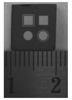
The 10 × 10 × 1.84 mm$^{3}$ fabricated CMT sample with 4 different front electrode configurations
SEMICONDUCTOR MATERIALS
R. Rafiei1, 2, , M.I. Reinhard1, A. Sarbutt1, S. Uxa3, D. Boardman1, G.C. Watt1, E. Belas3, K. Kim4, 5, A.E. Bolotnikov4 and R.B. James4
Corresponding author: R. Rafiei, Email:ramin.rafiei@uwa.edu.au
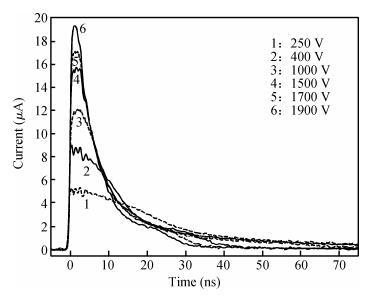
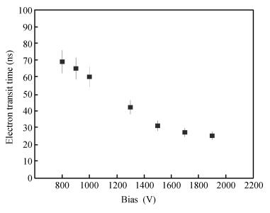
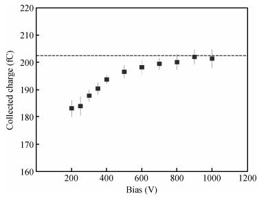
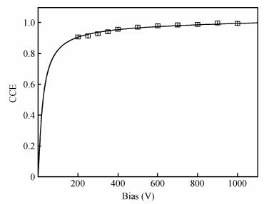
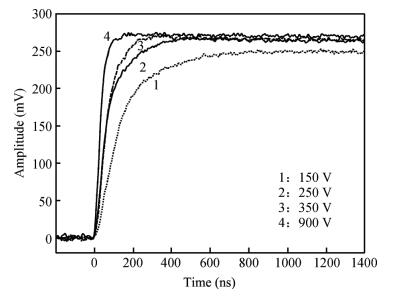
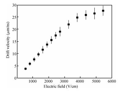
Abstract: Charge transport characteristics of Cd0.95Mn0.05Te:In radiation detectors have been evaluated by combining time resolved current transient measurements with time of flight charge transient measurements. The shapes of the measured current pulses have been interpreted with respect to a concentration of net positive space-charge, which has resulted in an electric field gradient across the detector bulk. From the recorded current pulses the charge collection efficiency of the detector was found to approach 100%. From the evolution of the charge collection efficiency with applied bias, the electron mobility-lifetime product of μnτn=(8.5±0.4)×10-4 cm2/V has been estimated. The electron transit time was determined using both transient current technique and time of flight measurements in the bias range of 100-1900 V. From the dependence of drift velocity on applied electric field the electron mobility was found to be μn=(718±55) cm2/(V·s) at room temperature.
Keywords: radiation detector, CdMnTe, CMT, detector fabrication, transient current technique, time of flight technique
| [1] |
Shockley W.Currents to conductors induced by a moving point charge.J Appl Phys, 1938, 9:635. doi: 10.1063/1.1710367
|
| [2] |
Ramo S.Currents induced by electron motion.Proc IRE, 1939, 27:584 doi: 10.1109/JRPROC.1939.228757
|
| [3] |
Shockley W, Pearson G L, Haynes R J.Hole injection in germanium-quantitative studies and filamentary transistors.Bell System Technical Journal, 1949, 28:344 doi: 10.1002/bltj.1949.28.issue-3
|
| [4] |
Quaranta A A, Martini M, Ottaviani G.Fast pulse pickoff with semiconductor radiation detectors.Nucl Inst Meth, 1967, 47:10 doi: 10.1016/0029-554X(67)90154-1
|
| [5] |
Quaranta A A, Cipolla F, Martini M.On a new method for measuring the charge carriers drift mobility in high resistivity silicon.Phys Lett, 1965, 17:102 doi: 10.1016/0031-9163(65)90254-4
|
| [6] |
Crandall R S.Trap spectroscopy of a-Si:H diodes using transient current techniques.J Electr Mater, 1980, 9:713 doi: 10.1007/BF02652892
|
| [7] |
Kraner H W, Li Z, Fretwurst E.The use of the signal current pulse shape to study the internal electric field profile and trapping effects in neutron damaged silicon detectors.Nucl Inst Meth A, 1993, 326:350 doi: 10.1016/0168-9002(93)90376-S
|
| [8] |
Bates A G, Moll M.A comparison between irradiated magnetic Czochralski and float zone silicon detectors using the transient current technique.Nucl Inst Meth A, 2005, 555:113. doi: 10.1016/j.nima.2005.09.020
|
| [9] |
Härkönen J, Ereminb V, Verbitskaya E, et al.The cryogenic transient current technique (C-TCT) measurement setup of CERN RD39 collaboration.Nucl Inst Meth A, 2007, 581:347 doi: 10.1016/j.nima.2007.08.001
|
| [10] |
Williams M L, Donnelly I J.An investigation of electric field behaviour in semi-insulating GaAs using current pulses.J Phys D:Appl Phys, 1996, 29:1997 doi: 10.1088/0022-3727/29/7/036
|
| [11] |
Fink J, Krüger H, Lodomez P, et al.Characterization of charge collection in CdTe and CZT using the transient current technique.Nucl Inst Meth A, 2006, 560:435 doi: 10.1016/j.nima.2006.01.072
|
| [12] |
Burshtein Z, Jayatirtha H N, Burger A, et al.Charge-carrier mobilities in Cd0.8Zn0.2Te single crystals used as nuclear radiation detectors.Appl Phys Lett, 1993, 63:102 doi: 10.1063/1.109726
|
| [13] |
Canali C, Gatti E, Kozlov S F, et al.Electrical properties and performances of natural diamond nuclear radiation detectors.Nucl Inst Meth, 1979, 160:73 doi: 10.1016/0029-554X(79)90167-8
|
| [14] |
Pernegger H, Roe S, Weilhammer P, et al.Charge-carrier properties in synthetic single-crystal diamond measured with the transient-current technique.J Appl Phys, 2005, 97:073704 doi: 10.1063/1.1863417
|
| [15] |
Isberg J, Gabrysch M, Tajani A, et al.Transient current electric field profiling of single crystal CVD diamond.Semicond Sci Technol, 2006, 21:1193 doi: 10.1088/0268-1242/21/8/035
|
| [16] |
Rafiei R, Boardman D, Sarbutt A, et al.Investigation of the charge collection efficiency of CdMnTe radiation detectors.IEEE Trans Nucl Sci, 2012, 59:634 doi: 10.1109/TNS.2012.2190941
|
| [17] |
Rafiei R, Boardman D, Sarbult A, et al.Charge transport properties of CdMnTe radiation detectors.EPJ Web of Conferences, 2012, 35:02005 doi: 10.1051/epjconf/20123502005
|
| [18] |
Mycielski A, Burger A, Sowinska M, et al.Is the (Cd, Mn) Te crystal a prospective material for X-ray and γ-ray detectors.Phys Status Solidi C, 2005, 2:1578 doi: 10.1002/(ISSN)1610-1642
|
| [19] |
Zhang J, Jie W, Wang T, et al.Growth and characterization of In doped Cd0.8Mn0.2Te single crystal.J Cryst Growth, 2007, 306:33 doi: 10.1016/j.jcrysgro.2007.03.044
|
| [20] |
Babalola O S, Bolotnikov A E, Groza M, et al.Study of Te inclusions in CdMnTe crystals for nuclear detector applications.J Cryst Growth, 2009, 311:3702 doi: 10.1016/j.jcrysgro.2009.04.037
|
| [21] |
Hossain A, Cui Y, Bolotnikov A E, et al.Vanadium-doped cadmium manganese telluride (Cd1-xMnxTe) crystals as X-and gamma-ray detectors.J Electron Mater, 2009, 38:1593 doi: 10.1007/s11664-009-0780-9
|
| [22] |
Kim K, Cho S, Suh J, et al.Gamma-ray response of semi-insulating CdMnTe crystals.IEEE Trans Nucl Sci, 2009, 56:858 doi: 10.1109/TNS.2009.2015662
|
| [23] |
Kim K H, Carcelén V, Bolotnikov A E, et al.Effective surface passivation of CdMnTe materials.J Electron Mater, 2010, 39:1015 doi: 10.1007/s11664-010-1090-y
|
| [24] |
Yang G, Bolotnikov A E, Li L, et al.Investigation of cadmium manganese telluride crystals for room-temperature radiation detection.J Electron Mater, 2010, 39:1053 doi: 10.1007/s11664-009-1050-6
|
| [25] |
Du Y, Jie W, Wang T, et al.Vertical Bridgman growth and characterization of CdMnTe crystals for gamma-ray radiation detector.J Cryst Growth, 2011, 318:1062 doi: 10.1016/j.jcrysgro.2010.11.086
|
| [26] |
Witkowska-Baran M, Mycielski A, Kochanowska D, et al.Amorphous contact layers on (Cd, Mn) Te crystals.J Cryst Growth, 2011, 320:1 doi: 10.1016/j.jcrysgro.2011.01.001
|
| [27] |
Witkowska-Baran M, Mycielski A, Kochanowska D, et al.Contacts for high-resistivity (Cd, Mn) Te crystals.IEEE Trans Nucl Sci, 2011, 58:347 doi: 10.1109/TNS.2010.2100827
|
| [28] |
Kim K H, Bolotinikov A E, Camarda G S, et al.Defect levels of semi-insulating CdMnTe:In crystals.J Appl Phys, 2011, 109:113715 doi: 10.1063/1.3594715
|
| [29] |
Ziegler J F.SRIM-2003.Nucl Inst Meth B, 2004, 219/220:1027 doi: 10.1016/j.nimb.2004.01.208
|
| [30] |
MATLAB version 7. 11. 0. Natick, Massachusetts: The MathWorks Inc. , 2010
|
| [31] |
Parkin J. Properties of Cd1-xMnxTe as a room temperature semiconductor radiation detector. PhD Thesis, Faculty of Eng and Phys Sci, Univ Surrey, Surrey, UK, 2009
|
| [32] |
Nemirovsky Y, Ruzin A, Asa G, et al.Study of the charge collection efficiency of CdZnTe radiation detectors.J Electron Mater, 1996, 25:1221 doi: 10.1007/BF02655012
|
| [33] |
Erickson J C, Yao H W, James R B, et al.Time of flight experimental studies of CdZnTe radiation detectors.J Electron Mater, 2000, 29:699 doi: 10.1007/s11664-000-0208-z
|
| [34] |
Eremin V, Li Z.Carrier drift mobility in neutron irradiated high purity silicon.Nucl Inst Meth A, 1995, 362:338 doi: 10.1016/0168-9002(95)00381-9
|
| [35] |
Roy U N, Weiler S, Stein J, et al.Charge transport properties of as-grown CZT by traveling heater method.Nucl Inst Meth A, 2011, 652:162 doi: 10.1016/j.nima.2011.01.143
|
| [36] |
Suzuki K, Seto S, Dairaku S, et al.Drift mobility and photoluminescence measurements on high resistivity Cd1-xZnxTe crystals grown from Te-rich solution.J Electron Mater, 1996, 25:1241 doi: 10.1007/BF02655014
|
| [37] |
Siegele R, Cohen D D, Dytlewski N.The ANSTO high energy heavy ion microprobe.Nucl Inst Meth B, 1999, 158:31 doi: 10.1016/S0168-583X(99)00393-6
|


Article views: 2703 Times PDF downloads: 20 Times Cited by: 0 Times
Received: 12 December 2012 Revised: 08 February 2013 Online: Published: 01 July 2013
| Citation: |
R. Rafiei, M.I. Reinhard, A. Sarbutt, S. Uxa, D. Boardman, G.C. Watt, E. Belas, K. Kim, A.E. Bolotnikov, R.B. James. Characterization of CdMnTe radiation detectors using current and charge transients[J]. Journal of Semiconductors, 2013, 34(7): 073001. doi: 10.1088/1674-4926/34/7/073001
****
R. Rafiei, M.I. Reinhard, A. Sarbutt, S. Uxa, D. Boardman, G.C. Watt, E. Belas, K. Kim, A.E. Bolotnikov, R.B. James. Characterization of CdMnTe radiation detectors using current and charge transients[J]. J. Semicond., 2013, 34(7): 073001. doi: 10.1088/1674-4926/34/7/073001.

|
| [1] |
Shockley W.Currents to conductors induced by a moving point charge.J Appl Phys, 1938, 9:635. doi: 10.1063/1.1710367
|
| [2] |
Ramo S.Currents induced by electron motion.Proc IRE, 1939, 27:584 doi: 10.1109/JRPROC.1939.228757
|
| [3] |
Shockley W, Pearson G L, Haynes R J.Hole injection in germanium-quantitative studies and filamentary transistors.Bell System Technical Journal, 1949, 28:344 doi: 10.1002/bltj.1949.28.issue-3
|
| [4] |
Quaranta A A, Martini M, Ottaviani G.Fast pulse pickoff with semiconductor radiation detectors.Nucl Inst Meth, 1967, 47:10 doi: 10.1016/0029-554X(67)90154-1
|
| [5] |
Quaranta A A, Cipolla F, Martini M.On a new method for measuring the charge carriers drift mobility in high resistivity silicon.Phys Lett, 1965, 17:102 doi: 10.1016/0031-9163(65)90254-4
|
| [6] |
Crandall R S.Trap spectroscopy of a-Si:H diodes using transient current techniques.J Electr Mater, 1980, 9:713 doi: 10.1007/BF02652892
|
| [7] |
Kraner H W, Li Z, Fretwurst E.The use of the signal current pulse shape to study the internal electric field profile and trapping effects in neutron damaged silicon detectors.Nucl Inst Meth A, 1993, 326:350 doi: 10.1016/0168-9002(93)90376-S
|
| [8] |
Bates A G, Moll M.A comparison between irradiated magnetic Czochralski and float zone silicon detectors using the transient current technique.Nucl Inst Meth A, 2005, 555:113. doi: 10.1016/j.nima.2005.09.020
|
| [9] |
Härkönen J, Ereminb V, Verbitskaya E, et al.The cryogenic transient current technique (C-TCT) measurement setup of CERN RD39 collaboration.Nucl Inst Meth A, 2007, 581:347 doi: 10.1016/j.nima.2007.08.001
|
| [10] |
Williams M L, Donnelly I J.An investigation of electric field behaviour in semi-insulating GaAs using current pulses.J Phys D:Appl Phys, 1996, 29:1997 doi: 10.1088/0022-3727/29/7/036
|
| [11] |
Fink J, Krüger H, Lodomez P, et al.Characterization of charge collection in CdTe and CZT using the transient current technique.Nucl Inst Meth A, 2006, 560:435 doi: 10.1016/j.nima.2006.01.072
|
| [12] |
Burshtein Z, Jayatirtha H N, Burger A, et al.Charge-carrier mobilities in Cd0.8Zn0.2Te single crystals used as nuclear radiation detectors.Appl Phys Lett, 1993, 63:102 doi: 10.1063/1.109726
|
| [13] |
Canali C, Gatti E, Kozlov S F, et al.Electrical properties and performances of natural diamond nuclear radiation detectors.Nucl Inst Meth, 1979, 160:73 doi: 10.1016/0029-554X(79)90167-8
|
| [14] |
Pernegger H, Roe S, Weilhammer P, et al.Charge-carrier properties in synthetic single-crystal diamond measured with the transient-current technique.J Appl Phys, 2005, 97:073704 doi: 10.1063/1.1863417
|
| [15] |
Isberg J, Gabrysch M, Tajani A, et al.Transient current electric field profiling of single crystal CVD diamond.Semicond Sci Technol, 2006, 21:1193 doi: 10.1088/0268-1242/21/8/035
|
| [16] |
Rafiei R, Boardman D, Sarbutt A, et al.Investigation of the charge collection efficiency of CdMnTe radiation detectors.IEEE Trans Nucl Sci, 2012, 59:634 doi: 10.1109/TNS.2012.2190941
|
| [17] |
Rafiei R, Boardman D, Sarbult A, et al.Charge transport properties of CdMnTe radiation detectors.EPJ Web of Conferences, 2012, 35:02005 doi: 10.1051/epjconf/20123502005
|
| [18] |
Mycielski A, Burger A, Sowinska M, et al.Is the (Cd, Mn) Te crystal a prospective material for X-ray and γ-ray detectors.Phys Status Solidi C, 2005, 2:1578 doi: 10.1002/(ISSN)1610-1642
|
| [19] |
Zhang J, Jie W, Wang T, et al.Growth and characterization of In doped Cd0.8Mn0.2Te single crystal.J Cryst Growth, 2007, 306:33 doi: 10.1016/j.jcrysgro.2007.03.044
|
| [20] |
Babalola O S, Bolotnikov A E, Groza M, et al.Study of Te inclusions in CdMnTe crystals for nuclear detector applications.J Cryst Growth, 2009, 311:3702 doi: 10.1016/j.jcrysgro.2009.04.037
|
| [21] |
Hossain A, Cui Y, Bolotnikov A E, et al.Vanadium-doped cadmium manganese telluride (Cd1-xMnxTe) crystals as X-and gamma-ray detectors.J Electron Mater, 2009, 38:1593 doi: 10.1007/s11664-009-0780-9
|
| [22] |
Kim K, Cho S, Suh J, et al.Gamma-ray response of semi-insulating CdMnTe crystals.IEEE Trans Nucl Sci, 2009, 56:858 doi: 10.1109/TNS.2009.2015662
|
| [23] |
Kim K H, Carcelén V, Bolotnikov A E, et al.Effective surface passivation of CdMnTe materials.J Electron Mater, 2010, 39:1015 doi: 10.1007/s11664-010-1090-y
|
| [24] |
Yang G, Bolotnikov A E, Li L, et al.Investigation of cadmium manganese telluride crystals for room-temperature radiation detection.J Electron Mater, 2010, 39:1053 doi: 10.1007/s11664-009-1050-6
|
| [25] |
Du Y, Jie W, Wang T, et al.Vertical Bridgman growth and characterization of CdMnTe crystals for gamma-ray radiation detector.J Cryst Growth, 2011, 318:1062 doi: 10.1016/j.jcrysgro.2010.11.086
|
| [26] |
Witkowska-Baran M, Mycielski A, Kochanowska D, et al.Amorphous contact layers on (Cd, Mn) Te crystals.J Cryst Growth, 2011, 320:1 doi: 10.1016/j.jcrysgro.2011.01.001
|
| [27] |
Witkowska-Baran M, Mycielski A, Kochanowska D, et al.Contacts for high-resistivity (Cd, Mn) Te crystals.IEEE Trans Nucl Sci, 2011, 58:347 doi: 10.1109/TNS.2010.2100827
|
| [28] |
Kim K H, Bolotinikov A E, Camarda G S, et al.Defect levels of semi-insulating CdMnTe:In crystals.J Appl Phys, 2011, 109:113715 doi: 10.1063/1.3594715
|
| [29] |
Ziegler J F.SRIM-2003.Nucl Inst Meth B, 2004, 219/220:1027 doi: 10.1016/j.nimb.2004.01.208
|
| [30] |
MATLAB version 7. 11. 0. Natick, Massachusetts: The MathWorks Inc. , 2010
|
| [31] |
Parkin J. Properties of Cd1-xMnxTe as a room temperature semiconductor radiation detector. PhD Thesis, Faculty of Eng and Phys Sci, Univ Surrey, Surrey, UK, 2009
|
| [32] |
Nemirovsky Y, Ruzin A, Asa G, et al.Study of the charge collection efficiency of CdZnTe radiation detectors.J Electron Mater, 1996, 25:1221 doi: 10.1007/BF02655012
|
| [33] |
Erickson J C, Yao H W, James R B, et al.Time of flight experimental studies of CdZnTe radiation detectors.J Electron Mater, 2000, 29:699 doi: 10.1007/s11664-000-0208-z
|
| [34] |
Eremin V, Li Z.Carrier drift mobility in neutron irradiated high purity silicon.Nucl Inst Meth A, 1995, 362:338 doi: 10.1016/0168-9002(95)00381-9
|
| [35] |
Roy U N, Weiler S, Stein J, et al.Charge transport properties of as-grown CZT by traveling heater method.Nucl Inst Meth A, 2011, 652:162 doi: 10.1016/j.nima.2011.01.143
|
| [36] |
Suzuki K, Seto S, Dairaku S, et al.Drift mobility and photoluminescence measurements on high resistivity Cd1-xZnxTe crystals grown from Te-rich solution.J Electron Mater, 1996, 25:1241 doi: 10.1007/BF02655014
|
| [37] |
Siegele R, Cohen D D, Dytlewski N.The ANSTO high energy heavy ion microprobe.Nucl Inst Meth B, 1999, 158:31 doi: 10.1016/S0168-583X(99)00393-6
|

 WeChat ID
Journal of Semiconductors © 2017 All Rights Reserved 京ICP备05085259号-2

 DownLoad: