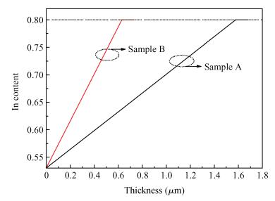
Fig. 1.
The indium composition versus growth thickness for samples A and B
SEMICONDUCTOR MATERIALS
Xiang Fang1, Yi Gu1, 2, Xingyou Chen1, Li Zhou1, Yuanying Cao1, Haosibaiyin Li1 and Yonggang Zhang1, 2,
Corresponding author: Zhang Yonggang, Email:ygzhang@mail.sim.ac.cn
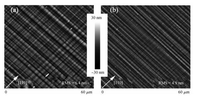
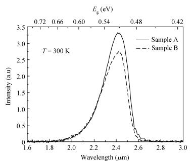
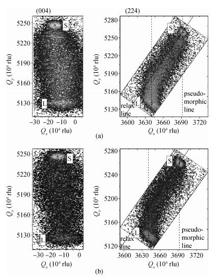
Abstract: Linearly graded InxGa1-xAs metamorphic buffers with different mismatch grading rates were grown on InP substrate by gas source molecular beam epitaxy. Room temperature photoluminescence spectra show that the sample with lower mismatch grading rate in the buffer has stronger photoluminescence signal, indicating the improved optical property. Atomic force microscope images show that the lower mismatch grading rate in the buffer leads to a slightly rougher surface. The relaxation procedure with two steps in the buffer layers has been observed by X-ray diffraction reciprocal space mapping. The measurements of X-ray diffraction also reveal that the lower mismatch grading rate in the buffer is beneficial for the lattice relaxation and release of residual strain. To further increase the relaxation degree, a lower mismatch grading rate and composition "overshoot" are suggested.
Keywords: InxGa1-xAs, gas source molecular beam epitaxy, photoluminescence, reciprocal space mapping
| [1] |
Chui H C, Lord S M, Martinet E, et al. Intersubband transitions in high indium content InGaAs/AlGaAs quantum wells. Appl Phys Lett, 1993, 63(3):364 doi: 10.1063/1.110044
|
| [2] |
Tångring I, Wang S M, Gu Q F, et al. Strong 1.3-1.6μm light emission from metamorphic InGaAs quantum wells on GaAs. Appl Phys Lett, 2005, 86(17):171902 doi: 10.1063/1.1906308
|
| [3] |
Tångring I, Ni H Q, Wu B P, et al. 1.58μm InGaAs quantum well laser on GaAs. Appl Phys Lett, 2007, 91(22):221101 doi: 10.1063/1.2803756
|
| [4] |
Wang H l, Wu D H, Wu B P, et al. Metamorphic InGaAs quantum well laser diodes at 1.5μm on GaAs grown by molecular beam epitaxy. Chin Phys Lett, 2009, 26(1):014214 doi: 10.1088/0256-307X/26/1/014214
|
| [5] |
Mogg S, Chitica N, Schatz R, et al. Properties of highly strained InGaAs/GaAs quantum wells for 1.2μm laser diodes. Appl Phys Lett, 2002, 81(13):2334 doi: 10.1063/1.1509478
|
| [6] |
Sundgren P, Berggren J, Goldman P, et al. Highly strained InGaAs/GaAs multiple quantum-wells for laser applications in the 1200-1300 nm wavelength regime. Appl Phys Lett, 2005, 87(7):071104 doi: 10.1063/1.2010615
|
| [7] |
Seravalli L, Trevisi G, Frigeri P, et al. Single quantum dot emission at telecom wavelengths from metamorphic InAs/InGaAs nanostructures grown on GaAs substrates. Appl Phys Lett, 2011, 98(17):173112 doi: 10.1063/1.3584132
|
| [8] |
Semenova E S, Zhukov A E, Mikhrin S S, et al. Metamorphic growth for application in long-wavelength (1.3-1.55μm) lasers and MODFET-type structures on GaAs substrates. Nanotechno-logy, 2004, 15(4):S283 doi: 10.1088/0957-4484/15/4/031
|
| [9] |
Seravalli L, Frigeri P, Nasi L, et al. Metamorphic quantum dots:quite different nanostructures. J Appl Phys, 2010, 108(6):064324 doi: 10.1063/1.3483249
|
| [10] |
Behet M, Van der Zanden K, Borghs G, et al. Metamorphic InGaAs/InAlAs quantum well structures grown on GaAs substrates for high electron mobility transistor applications. Appl Phys Lett, 1998, 73(19):2760 doi: 10.1063/1.122582
|
| [11] |
Win P, Druelle Y, Cappy A, et al. Metamorphic In0.3Ga0.7As/In0.29Al0.71As layer on GaAs:a new structure for high performance high electron mobility transistor realization. Appl Phys Lett, 1992, 61(8):922 doi: 10.1063/1.107729
|
| [12] |
Zhang Y G, Gu Y, Tian Z B, et al. Performance of gas source MBE-grown wavelength extended InGaAs photodetectors with different buffer structures. J Crystal Growth, 2009, 311(7):1881 doi: 10.1016/j.jcrysgro.2008.10.087
|
| [13] |
Gu Y, Wang K, Li C, et al. High indium content InGaAs photodetector:with InGaAs or InAlAs graded buffer layers. J Infrared Millim Waves, 2011, 30(6):481
|
| [14] |
Zhang Y G, Gu Y, Tian Z B, et al. Wavelength extended 2.4μm heterojunction InGaAs photodiodes with InAlAs cap and linearly graded buffer layers suitable for both front and back illuminations. Infrared Physics and Technology, 2008, 51(4):316
|
| [15] |
Gu Y, Zhang Y G, Wang K, et al. InP-based InAs/InGaAs quantum wells with type-I emission beyond 3μm. Appl Phys Lett, 2011, 99(8):081914 doi: 10.1063/1.3629999
|
| [16] |
Zhang Y G, Gu Y, Wang K, et, al. Fourier transform infrared spectroscopy approach for measurements of photoluminescence and electroluminescence in mid-infrared. Rev Sci Instrum, 2012, 83(5):053106 doi: 10.1063/1.4717673
|
| [17] |
Wang S M, Karlsson C, Rorsman N, et al. Molecular beam epitaxy growth and characterization of InxGa1-xAs (0.57 < x < 1) on GaAs using InAlAs graded buffer. J Crystal Growth, 1997, 175/176(5):1016
|
| [18] |
Tersoff J. Dislocations and strain relief in compositionally graded layers. Appl Phys Lett, 1993, 62(7):693 doi: 10.1063/1.108842
|
| [19] |
Dunstan D J, Kidd P, Howard L K, et al. Plastic relaxation of InGaAs grown on GaAs. Appl Phys Lett, 1991, 59(26):3390 doi: 10.1063/1.105684
|
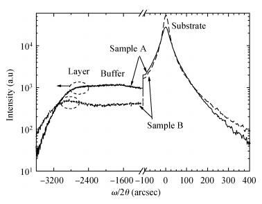
Table 1. Results extracted from the RSM measurements

|
| [1] |
Chui H C, Lord S M, Martinet E, et al. Intersubband transitions in high indium content InGaAs/AlGaAs quantum wells. Appl Phys Lett, 1993, 63(3):364 doi: 10.1063/1.110044
|
| [2] |
Tångring I, Wang S M, Gu Q F, et al. Strong 1.3-1.6μm light emission from metamorphic InGaAs quantum wells on GaAs. Appl Phys Lett, 2005, 86(17):171902 doi: 10.1063/1.1906308
|
| [3] |
Tångring I, Ni H Q, Wu B P, et al. 1.58μm InGaAs quantum well laser on GaAs. Appl Phys Lett, 2007, 91(22):221101 doi: 10.1063/1.2803756
|
| [4] |
Wang H l, Wu D H, Wu B P, et al. Metamorphic InGaAs quantum well laser diodes at 1.5μm on GaAs grown by molecular beam epitaxy. Chin Phys Lett, 2009, 26(1):014214 doi: 10.1088/0256-307X/26/1/014214
|
| [5] |
Mogg S, Chitica N, Schatz R, et al. Properties of highly strained InGaAs/GaAs quantum wells for 1.2μm laser diodes. Appl Phys Lett, 2002, 81(13):2334 doi: 10.1063/1.1509478
|
| [6] |
Sundgren P, Berggren J, Goldman P, et al. Highly strained InGaAs/GaAs multiple quantum-wells for laser applications in the 1200-1300 nm wavelength regime. Appl Phys Lett, 2005, 87(7):071104 doi: 10.1063/1.2010615
|
| [7] |
Seravalli L, Trevisi G, Frigeri P, et al. Single quantum dot emission at telecom wavelengths from metamorphic InAs/InGaAs nanostructures grown on GaAs substrates. Appl Phys Lett, 2011, 98(17):173112 doi: 10.1063/1.3584132
|
| [8] |
Semenova E S, Zhukov A E, Mikhrin S S, et al. Metamorphic growth for application in long-wavelength (1.3-1.55μm) lasers and MODFET-type structures on GaAs substrates. Nanotechno-logy, 2004, 15(4):S283 doi: 10.1088/0957-4484/15/4/031
|
| [9] |
Seravalli L, Frigeri P, Nasi L, et al. Metamorphic quantum dots:quite different nanostructures. J Appl Phys, 2010, 108(6):064324 doi: 10.1063/1.3483249
|
| [10] |
Behet M, Van der Zanden K, Borghs G, et al. Metamorphic InGaAs/InAlAs quantum well structures grown on GaAs substrates for high electron mobility transistor applications. Appl Phys Lett, 1998, 73(19):2760 doi: 10.1063/1.122582
|
| [11] |
Win P, Druelle Y, Cappy A, et al. Metamorphic In0.3Ga0.7As/In0.29Al0.71As layer on GaAs:a new structure for high performance high electron mobility transistor realization. Appl Phys Lett, 1992, 61(8):922 doi: 10.1063/1.107729
|
| [12] |
Zhang Y G, Gu Y, Tian Z B, et al. Performance of gas source MBE-grown wavelength extended InGaAs photodetectors with different buffer structures. J Crystal Growth, 2009, 311(7):1881 doi: 10.1016/j.jcrysgro.2008.10.087
|
| [13] |
Gu Y, Wang K, Li C, et al. High indium content InGaAs photodetector:with InGaAs or InAlAs graded buffer layers. J Infrared Millim Waves, 2011, 30(6):481
|
| [14] |
Zhang Y G, Gu Y, Tian Z B, et al. Wavelength extended 2.4μm heterojunction InGaAs photodiodes with InAlAs cap and linearly graded buffer layers suitable for both front and back illuminations. Infrared Physics and Technology, 2008, 51(4):316
|
| [15] |
Gu Y, Zhang Y G, Wang K, et al. InP-based InAs/InGaAs quantum wells with type-I emission beyond 3μm. Appl Phys Lett, 2011, 99(8):081914 doi: 10.1063/1.3629999
|
| [16] |
Zhang Y G, Gu Y, Wang K, et, al. Fourier transform infrared spectroscopy approach for measurements of photoluminescence and electroluminescence in mid-infrared. Rev Sci Instrum, 2012, 83(5):053106 doi: 10.1063/1.4717673
|
| [17] |
Wang S M, Karlsson C, Rorsman N, et al. Molecular beam epitaxy growth and characterization of InxGa1-xAs (0.57 < x < 1) on GaAs using InAlAs graded buffer. J Crystal Growth, 1997, 175/176(5):1016
|
| [18] |
Tersoff J. Dislocations and strain relief in compositionally graded layers. Appl Phys Lett, 1993, 62(7):693 doi: 10.1063/1.108842
|
| [19] |
Dunstan D J, Kidd P, Howard L K, et al. Plastic relaxation of InGaAs grown on GaAs. Appl Phys Lett, 1991, 59(26):3390 doi: 10.1063/1.105684
|


Article views: 2595 Times PDF downloads: 21 Times Cited by: 0 Times
Received: 08 November 2012 Revised: 11 December 2012 Online: Published: 01 July 2013
| Citation: |
Xiang Fang, Yi Gu, Xingyou Chen, Li Zhou, Yuanying Cao, Haosibaiyin Li, Yonggang Zhang. InP-based InxGa1-xAs metamorphic buffers with different mismatch grading rates[J]. Journal of Semiconductors, 2013, 34(7): 073005. doi: 10.1088/1674-4926/34/7/073005
****
X Fang, Y Gu, X Y Chen, L Zhou, Y Y Cao, H S B Y Li, Y G Zhang. InP-based InxGa1-xAs metamorphic buffers with different mismatch grading rates[J]. J. Semicond., 2013, 34(7): 073005. doi: 10.1088/1674-4926/34/7/073005.

|
| [1] |
Chui H C, Lord S M, Martinet E, et al. Intersubband transitions in high indium content InGaAs/AlGaAs quantum wells. Appl Phys Lett, 1993, 63(3):364 doi: 10.1063/1.110044
|
| [2] |
Tångring I, Wang S M, Gu Q F, et al. Strong 1.3-1.6μm light emission from metamorphic InGaAs quantum wells on GaAs. Appl Phys Lett, 2005, 86(17):171902 doi: 10.1063/1.1906308
|
| [3] |
Tångring I, Ni H Q, Wu B P, et al. 1.58μm InGaAs quantum well laser on GaAs. Appl Phys Lett, 2007, 91(22):221101 doi: 10.1063/1.2803756
|
| [4] |
Wang H l, Wu D H, Wu B P, et al. Metamorphic InGaAs quantum well laser diodes at 1.5μm on GaAs grown by molecular beam epitaxy. Chin Phys Lett, 2009, 26(1):014214 doi: 10.1088/0256-307X/26/1/014214
|
| [5] |
Mogg S, Chitica N, Schatz R, et al. Properties of highly strained InGaAs/GaAs quantum wells for 1.2μm laser diodes. Appl Phys Lett, 2002, 81(13):2334 doi: 10.1063/1.1509478
|
| [6] |
Sundgren P, Berggren J, Goldman P, et al. Highly strained InGaAs/GaAs multiple quantum-wells for laser applications in the 1200-1300 nm wavelength regime. Appl Phys Lett, 2005, 87(7):071104 doi: 10.1063/1.2010615
|
| [7] |
Seravalli L, Trevisi G, Frigeri P, et al. Single quantum dot emission at telecom wavelengths from metamorphic InAs/InGaAs nanostructures grown on GaAs substrates. Appl Phys Lett, 2011, 98(17):173112 doi: 10.1063/1.3584132
|
| [8] |
Semenova E S, Zhukov A E, Mikhrin S S, et al. Metamorphic growth for application in long-wavelength (1.3-1.55μm) lasers and MODFET-type structures on GaAs substrates. Nanotechno-logy, 2004, 15(4):S283 doi: 10.1088/0957-4484/15/4/031
|
| [9] |
Seravalli L, Frigeri P, Nasi L, et al. Metamorphic quantum dots:quite different nanostructures. J Appl Phys, 2010, 108(6):064324 doi: 10.1063/1.3483249
|
| [10] |
Behet M, Van der Zanden K, Borghs G, et al. Metamorphic InGaAs/InAlAs quantum well structures grown on GaAs substrates for high electron mobility transistor applications. Appl Phys Lett, 1998, 73(19):2760 doi: 10.1063/1.122582
|
| [11] |
Win P, Druelle Y, Cappy A, et al. Metamorphic In0.3Ga0.7As/In0.29Al0.71As layer on GaAs:a new structure for high performance high electron mobility transistor realization. Appl Phys Lett, 1992, 61(8):922 doi: 10.1063/1.107729
|
| [12] |
Zhang Y G, Gu Y, Tian Z B, et al. Performance of gas source MBE-grown wavelength extended InGaAs photodetectors with different buffer structures. J Crystal Growth, 2009, 311(7):1881 doi: 10.1016/j.jcrysgro.2008.10.087
|
| [13] |
Gu Y, Wang K, Li C, et al. High indium content InGaAs photodetector:with InGaAs or InAlAs graded buffer layers. J Infrared Millim Waves, 2011, 30(6):481
|
| [14] |
Zhang Y G, Gu Y, Tian Z B, et al. Wavelength extended 2.4μm heterojunction InGaAs photodiodes with InAlAs cap and linearly graded buffer layers suitable for both front and back illuminations. Infrared Physics and Technology, 2008, 51(4):316
|
| [15] |
Gu Y, Zhang Y G, Wang K, et al. InP-based InAs/InGaAs quantum wells with type-I emission beyond 3μm. Appl Phys Lett, 2011, 99(8):081914 doi: 10.1063/1.3629999
|
| [16] |
Zhang Y G, Gu Y, Wang K, et, al. Fourier transform infrared spectroscopy approach for measurements of photoluminescence and electroluminescence in mid-infrared. Rev Sci Instrum, 2012, 83(5):053106 doi: 10.1063/1.4717673
|
| [17] |
Wang S M, Karlsson C, Rorsman N, et al. Molecular beam epitaxy growth and characterization of InxGa1-xAs (0.57 < x < 1) on GaAs using InAlAs graded buffer. J Crystal Growth, 1997, 175/176(5):1016
|
| [18] |
Tersoff J. Dislocations and strain relief in compositionally graded layers. Appl Phys Lett, 1993, 62(7):693 doi: 10.1063/1.108842
|
| [19] |
Dunstan D J, Kidd P, Howard L K, et al. Plastic relaxation of InGaAs grown on GaAs. Appl Phys Lett, 1991, 59(26):3390 doi: 10.1063/1.105684
|

 WeChat ID
Journal of Semiconductors © 2017 All Rights Reserved 京ICP备05085259号-2

 DownLoad: