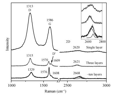
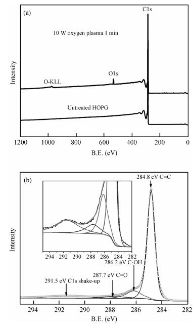
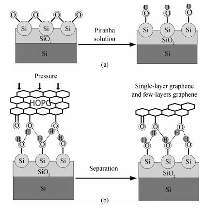
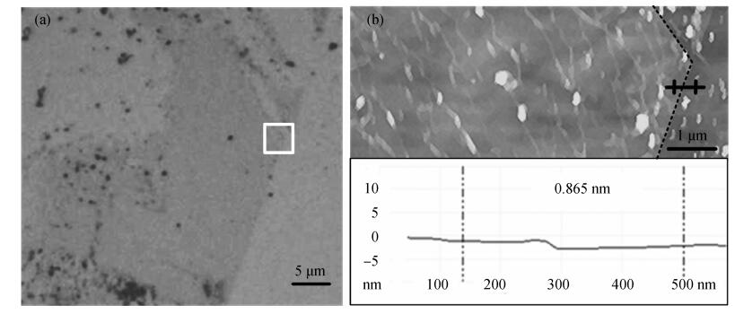
| [1] |
Soldano C, Mahmood A, Dujardin E. Production, properties and potential of graphene. Carbon, 2010, 48(8):2127 doi: 10.1016/j.carbon.2010.01.058 |
| [2] |
Geim A K, Novoselov K S. The rise of graphene. Nat Mater, 2007, 6(3):183 doi: 10.1038/nmat1849 |
| [3] |
Loh K P, Bao Q, Ang P K, et al. The chemistry of graphene. J Mater Chem, 2010, 20(12):2277 doi: 10.1039/b920539j |
| [4] |
Novoselov K, Geim A, Morozov S, et al. Electric field effect in atomically thin carbon films. Science, 2004, 306(5696):666 doi: 10.1126/science.1102896 |
| [5] |
Wang D C, Zhang Y M, Zhang Y M, et al. Raman analysis of epitaxial graphene on 6H-SiC (0001) substrates under low pressure environment. Journal of Semiconductors, 2011, 32(11):113003 doi: 10.1088/1674-4926/32/11/113003 |
| [6] |
|
| [7] |
Yuan G D, Zhang W J, Yang Y, et al. Graphene sheets via microwave chemical vapor deposition. Chem Phys Lett, 2009, 467(4-6):361 doi: 10.1016/j.cplett.2008.11.059 |
| [8] |
Zhao G, Shao D, Chen C, et al. Synthesis of few-layered graphene by H2O2 plasma etching of graphite. Appl Phys Lett, 2011, 98(18):183114 doi: 10.1063/1.3589354 |
| [9] |
Wang Y J, Miao C Q, Huang B C, et al. Scalable synthesis of graphene on patterned Ni and transfer. IEEE Trans Electron Devices, 2010, 57(12):3472 doi: 10.1109/TED.2010.2076337 |
| [10] |
Gao L, Ren W, Xu H, et al. Repeated growth and bubbling transfer of graphene with millimetre-size single-crystal grains using platinum. Nat Commun, 2012, 3:699 doi: 10.1038/ncomms1702 |
| [11] |
Huc V, Bendiab N, Rosman N, et al. Large and flat graphene flakes produced by epoxy bonding and reverse exfoliation of highly oriented pyrolytic graphite. Nanotechnology, 2008, 19(45):455601 doi: 10.1088/0957-4484/19/45/455601 |
| [12] |
Liang X, Fu Z, Chou S Y. Graphene transistors fabricated via transfer-printing in device active-areas on large wafer. Nano Lett, 2007, 7(12):3840 doi: 10.1021/nl072566s |
| [13] |
|
| [14] |
Liu L H, Yan M. Simple method for the covalent immobilization of graphene. Nano Lett, 2009, 9(9):3375 doi: 10.1021/nl901669h |
| [15] |
Goler S, Piazza V, Roddaro S, et al. Self-assembly and electron-beam-induced direct etching of suspended graphene nanostructures. J Appl Phys, 2011, 110(6):064308 doi: 10.1063/1.3633260 |
| [16] |
Nakahara M, Sanada Y. Modification of pyrolytic graphite surface with plasma irradiation. J Mater Sci, 1993, 28(5):1327 doi: 10.1007/BF01191973 |
| [17] |
Evans J F, Kuwana. Radiofrequency oxygen plasma treatment of pyrolytic graphite electrode surfaces. Anal Chem, 1977, 49(11):1632 doi: 10.1021/ac50019a042 |
| [18] |
Cvelbar U, Markoli B, Poberaj I, et al. Formation of functional groups on graphite during oxygen plasma treatment. Appl Surf Sci, 2006, 253(4):1861 doi: 10.1016/j.apsusc.2006.03.028 |
| [19] |
You H X, Brown N, Al-Assadi K, et al. Surface characterization of highly oriented pyrolytic graphite modified by oxygen radio-frequency plasmas. J Mater Sci Lett, 1993, 12(4):201 doi: 10.1007/BF00539797 |
| [20] |
Seah C M, Chai S P, Ichikawa S, et al. Synthesis of single-walled carbon nanotubes over a spin-coated Fe catalyst in an ethanol-PEG colloidal solution. Carbon, 2012, 50(3):960 doi: 10.1016/j.carbon.2011.09.059 |
| [21] |
Sabio J, Seoánez C, Fratini S, et al. Electrostatic interactions between graphene layers and their environment. Phys Rev B, 2008, 77(19):195409 doi: 10.1103/PhysRevB.77.195409 |
| [22] |
Ni Z H, Wang H M, Ma Y, et al. Tunable stress and controlled thickness modification in graphene by annealing. Acs Nano, 2008, 2(5):1033 doi: 10.1021/nn800031m |
| [23] |
Martins Ferreira E H, Moutinho M V O, Stavale F, et al. Evolution of the Raman spectra from single-, few-, and many-layer graphene with increasing disorder. Phys Rev B, 2010, 82(12):125429 doi: 10.1103/PhysRevB.82.125429 |
| [24] |
Ferrari A C, Meyer J C, Scardaci V, et al. Raman spectrum of graphene and graphene layers. Phys Rev Lett, 2006, 97(18):187401 doi: 10.1103/PhysRevLett.97.187401 |
| [25] |
Nakahara M, Sanada Y. Structural changes of a pyrolytic graphite surface oxidized by electrochemical and plasma treatment. J Mater Sci, 1994, 29(12):3193 doi: 10.1007/BF00356662 |
| [26] |
Kim Y Y, Lim W S, Park J B, et al. Layer by layer etching of the highly oriented pyrolythic graphite by using atomic layer etching. J Electrochem Soc, 2011, 158(12):D710 doi: 10.1149/2.061112jes |
| [27] |
Dieckhoff S, Schlett V, Possart W, et al. XPS studies of thin polycyanurate films on silicon wafers. Fresenius J Anal Chem, 1995, 353(3/4):278 doi: 10.1007%2FBF00322052.pdf |
| [28] |
Nagashio K, Yamashita T, Nishimura T, et al. Electrical transport properties of graphene on SiO 2 with specific surface structures. J Appl Phys, 2011, 110(2):024513 doi: 10.1063/1.3611394 |
| [29] |
Zhang Y, Small J P, Pontius W V, et al. Fabrication and electric-field-dependent transport measurements of mesoscopic graphite devices. Appl Phys Lett, 2005, 86(7):073104 doi: 10.1063/1.1862334 |


 DownLoad: