


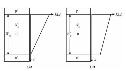
Fig. 1.
Cross-sectional structures and their electric field profiles $E(x)$ . (a) The NPT abrupt parallel-plane junctions. (b) The PT abrupt parallel-plane junctions.
SEMICONDUCTOR DEVICES
Corresponding author: Huang Haimeng, Email:haimenghuang@126.com
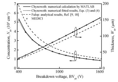
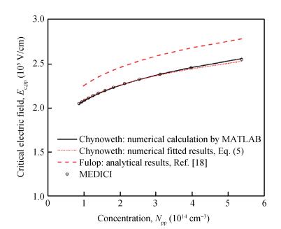
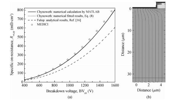
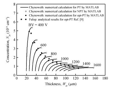
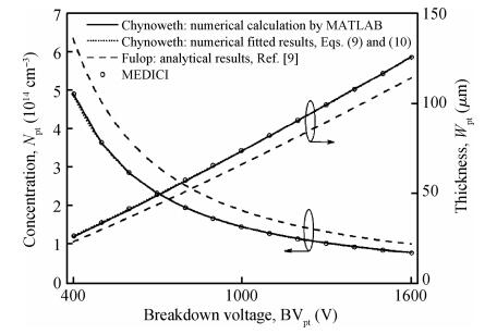
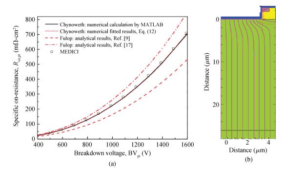
Abstract: The relations among the breakdown voltage, the width and the concentration of the voltage-sustaining layer for the non-punch-through (NPT) and punch-through (PT) abrupt parallel-plane junctions have been re-established based on the ionization integral by the Chynoweth model, distinguished from the conventional results obtained by the Fulop model. The numerical calculation results indicate that the new expressions are more accurate than those in previous literature. While the breakdown voltage of the NPT case varied from 400 to 1600 V using the Chynoweth model, the value using the Fulop model is overestimated by 12% (478 V) to 18% (1895 V). For the PT case with optimum design of the specific on-resistance, when the breakdown voltage is varied from 400 to 1600 V, the width and concentration are from 81.0168% to 80.2416% and from 91.4341% to 91.6941% of those of the NPT cases, respectively. The relations between the specific on-resistance and the breakdown voltage for both the NPT and PT structures are also established. Simulation results by MEDICI show good agreement with the proposed expressions.
Keywords: abrupt parallel-plane junction, impact ionization integral, Chynoweth law, Fulop law
| [1] |
Hu C. Optimum doping profile for minimum ohmic resistance and high-breakdown voltage. IEEE Trans Electron Devices, 1979, 26(3):243 doi: 10.1109/T-ED.1979.19416
|
| [2] |
Sun S C, Plummer J D. Modeling of the on-resistance of LDMOS, VDMOS, and VMOS power transistors. IEEE Trans Electron Devices, 1980, 27(2):356 doi: 10.1109/T-ED.1980.19868
|
| [3] |
Chen X, Hu C. Optimum doping profile of power MOSFET epitaxial layer. IEEE Trans Electron Devices, 1982, 29(6):2985
|
| [4] |
Darwish MN, Board K. Optimization of breakdown voltage and on-resistance of VDMOS transistors. IEEE Trans Electron Devices, 1984, 31(12):1769 doi: 10.1109/T-ED.1984.21786
|
| [5] |
Hu C, Chi M, Patel V M. Optimum design of power MOSFET's. IEEE Trans Electron Devices, 1984, 31(12):1693 doi: 10.1109/T-ED.1984.21773
|
| [6] |
Tarng M L. On-resistance characterization of VDMOS power transistors. Proc IEDM, 1981, (27):429 https://www.infona.pl/resource/bwmeta1.element.ieee-art-000004644319
|
| [7] |
Board K, Byrne D J, Towers M S. The optimization of on-resistance in vertical DMOS power devices with linear and hexagonal surface geometries. IEEE Trans Electron Devices, 1984, 31(1):75 doi: 10.1109/T-ED.1984.21476
|
| [8] |
Fernandez J, Hidalgo S, Paredes J, et al. An ON-resistance closed form for VDMOS devices. IEEE Electron Device Lett, 1989, 10(5):212 doi: 10.1109/55.31724
|
| [9] |
He J, Wang X, Chen X. Optimum design of epitaxial layers with uniform doping for VDMOS transistor. Chinese Journal of Semiconductors, 1999, 29(11):977
|
| [10] |
Fulop W. Calculation of avalanche breakdown voltages of silicon p-n junctions. Solid-State Electron, 1967, 10(1):39 doi: 10.1016/0038-1101(67)90111-6
|
| [11] |
Chynoweth A G. Ionization rates for electrons and holes in silicon. Phys Rev, 1958, 109(5):1537 doi: 10.1103/PhysRev.109.1537
|
| [12] |
Van Overstraeten R, de Man H. Measurement of the ionization rates in diffused silicon p-n junctions. Solid-State Electron, 1970, 13(5):583 doi: 10.1016/0038-1101(70)90139-5
|
| [13] |
Huang H, Chen X. Optimization of specific on-resistance of balanced symmetric superjunction MOSFETs based on a better approximation of ionization integral. IEEE Trans Electron Devices, 2012, 59(10):2742 doi: 10.1109/TED.2012.2207961
|
| [14] |
Caughey D, Thomas R. Carrier mobilities in silicon empirically related to doping and field. Proc IEEE, 1967:2192 http://citeseerx.ist.psu.edu/showciting?cid=1612830
|
| [15] |
MEDICI. Two dimensional device simulation program. ed. 2002. 2. 0, Synopsys Inc. , Fremont, CA, 2002
|
| [16] |
Baliga B J. Fundamentals of power semiconductor devices. New York:Springer-Verlag, 2008
|
| [17] |
Chen X. Theory of a novel voltage-sustaining composite buffer (CB) layer for power devices. Chin J Electron, 1998, 7(3):211 doi: 10.1007/s10825-016-0942-y
|
| [18] |
Baliga B J, Ghandhi S K. Analytical solutions for the breakdown voltage of abrupt cylindrical and spherical junctions. Solid-State Electron, 1976, 19:739 doi: 10.1016/0038-1101(76)90152-0
|


Article views: 3108 Times PDF downloads: 28 Times Cited by: 0 Times
Received: 01 November 2012 Revised: 30 January 2013 Online: Published: 01 July 2013
| Citation: |
Haimeng Huang, Xingbi Chen. New expressions for non-punch-through and punch-through abrupt parallel-plane junctions based on Chynoweth law[J]. Journal of Semiconductors, 2013, 34(7): 074003. doi: 10.1088/1674-4926/34/7/074003
****
H M Huang, X B Chen. New expressions for non-punch-through and punch-through abrupt parallel-plane junctions based on Chynoweth law[J]. J. Semicond., 2013, 34(7): 074003. doi: 10.1088/1674-4926/34/7/074003.

|
| [1] |
Hu C. Optimum doping profile for minimum ohmic resistance and high-breakdown voltage. IEEE Trans Electron Devices, 1979, 26(3):243 doi: 10.1109/T-ED.1979.19416
|
| [2] |
Sun S C, Plummer J D. Modeling of the on-resistance of LDMOS, VDMOS, and VMOS power transistors. IEEE Trans Electron Devices, 1980, 27(2):356 doi: 10.1109/T-ED.1980.19868
|
| [3] |
Chen X, Hu C. Optimum doping profile of power MOSFET epitaxial layer. IEEE Trans Electron Devices, 1982, 29(6):2985
|
| [4] |
Darwish MN, Board K. Optimization of breakdown voltage and on-resistance of VDMOS transistors. IEEE Trans Electron Devices, 1984, 31(12):1769 doi: 10.1109/T-ED.1984.21786
|
| [5] |
Hu C, Chi M, Patel V M. Optimum design of power MOSFET's. IEEE Trans Electron Devices, 1984, 31(12):1693 doi: 10.1109/T-ED.1984.21773
|
| [6] |
Tarng M L. On-resistance characterization of VDMOS power transistors. Proc IEDM, 1981, (27):429 https://www.infona.pl/resource/bwmeta1.element.ieee-art-000004644319
|
| [7] |
Board K, Byrne D J, Towers M S. The optimization of on-resistance in vertical DMOS power devices with linear and hexagonal surface geometries. IEEE Trans Electron Devices, 1984, 31(1):75 doi: 10.1109/T-ED.1984.21476
|
| [8] |
Fernandez J, Hidalgo S, Paredes J, et al. An ON-resistance closed form for VDMOS devices. IEEE Electron Device Lett, 1989, 10(5):212 doi: 10.1109/55.31724
|
| [9] |
He J, Wang X, Chen X. Optimum design of epitaxial layers with uniform doping for VDMOS transistor. Chinese Journal of Semiconductors, 1999, 29(11):977
|
| [10] |
Fulop W. Calculation of avalanche breakdown voltages of silicon p-n junctions. Solid-State Electron, 1967, 10(1):39 doi: 10.1016/0038-1101(67)90111-6
|
| [11] |
Chynoweth A G. Ionization rates for electrons and holes in silicon. Phys Rev, 1958, 109(5):1537 doi: 10.1103/PhysRev.109.1537
|
| [12] |
Van Overstraeten R, de Man H. Measurement of the ionization rates in diffused silicon p-n junctions. Solid-State Electron, 1970, 13(5):583 doi: 10.1016/0038-1101(70)90139-5
|
| [13] |
Huang H, Chen X. Optimization of specific on-resistance of balanced symmetric superjunction MOSFETs based on a better approximation of ionization integral. IEEE Trans Electron Devices, 2012, 59(10):2742 doi: 10.1109/TED.2012.2207961
|
| [14] |
Caughey D, Thomas R. Carrier mobilities in silicon empirically related to doping and field. Proc IEEE, 1967:2192 http://citeseerx.ist.psu.edu/showciting?cid=1612830
|
| [15] |
MEDICI. Two dimensional device simulation program. ed. 2002. 2. 0, Synopsys Inc. , Fremont, CA, 2002
|
| [16] |
Baliga B J. Fundamentals of power semiconductor devices. New York:Springer-Verlag, 2008
|
| [17] |
Chen X. Theory of a novel voltage-sustaining composite buffer (CB) layer for power devices. Chin J Electron, 1998, 7(3):211 doi: 10.1007/s10825-016-0942-y
|
| [18] |
Baliga B J, Ghandhi S K. Analytical solutions for the breakdown voltage of abrupt cylindrical and spherical junctions. Solid-State Electron, 1976, 19:739 doi: 10.1016/0038-1101(76)90152-0
|

 WeChat ID
Journal of Semiconductors © 2017 All Rights Reserved 京ICP备05085259号-2

 DownLoad:

