


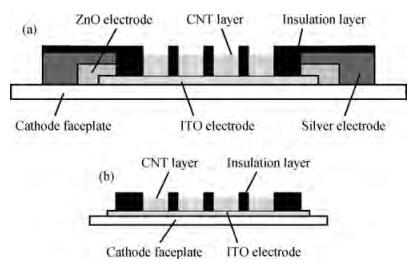
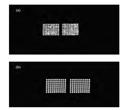
Fig. 1.
The structural schematic diagram of (a) the sandwich layered cathode electrode and (b) a common conducting electrode.
SEMICONDUCTOR DEVICES
Yukui Li1, , Xiaoquan Li1, Xinghui Liu2, Wenke Lu3 and Fanguang Zeng4
Corresponding author: Li Yukui, Email:lyksound@163.com
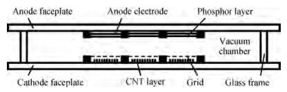
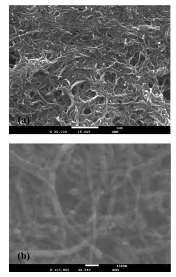
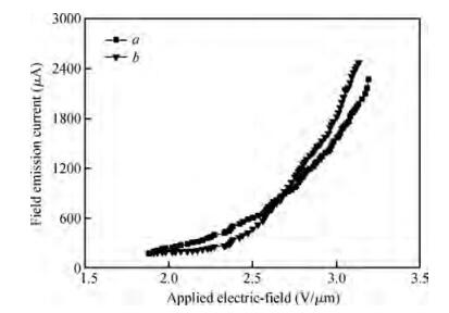
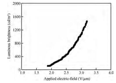
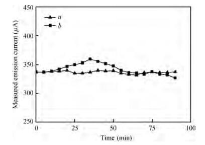
Abstract: Based on an effective screen-printing process, a novel sandwich layered cathode electrode was developed on a cathode faceplate. The ZnO electrode was sandwiched between an indium tin oxide (ITO) electrode layer and a silver electrode layer, and the carbon nanotube was prepared directly on the exposed ITO electrode layer surface. The cathode potential could be conducted to the carbon nanotube with the sandwich layered cathode electrode. Using the carbon nanotube as a field emitter, a triode field emission display prototype with a sandwich layered cathode electrode was fabricated, which possessed a better field emission characteristic, higher luminous brightness and better emission image luminance uniformity. The turn-on electric field was 1.88 V/μm and the measured maximum field emission current was 2273.6 μA at 3.19 V/μm. By the method of adjusting the field emission current, the electron-emitting uniform capacity of the carbon nanotube cold cathode could be modified, and the emission image luminance uniformity and the emission current stability of triode field emission display prototype was also be improved significantly. The emission current fluctuation of the sandwich layered cathode electrode type field emission display was less than 1.1%. Furthermore, the total manufacture cost of the triode field emission display prototype was low.
Keywords: cathode electrode, fabrication, screen-printing, field emission, sintering
| [1] |
Lee J, Jung Y, Song J, et al. High-performance field emission from a carbon nanotube carpet. Carbon, 2012, 50(10):3889 doi: 10.1016/j.carbon.2012.04.033
|
| [2] |
Cho W S, Lee Y D, Choi J, et al. Effects on the field emission properties by variation in surface morphology of patterned photo-sensitive carbon nanotube paste using organic solvent. Appl Surf Sci, 2011, 257(6):2250 doi: 10.1016/j.apsusc.2010.09.082
|
| [3] |
Zheng Longwu, Hu Liqin, Yang Fan, et al. Improvement of the field emission properties of carbon nanotubes by CNT/Fe3O4 composite electrophoretic deposition. Journal of Semiconductors, 2011, 32(12):126001 doi: 10.1088/1674-4926/32/12/126001
|
| [4] |
Neupane S, Lastres M, Chiarella M, et al. Synthesis and field emission properties of vertically aligned carbon nanotube arrays on copper. Carbon, 2012, 50(7):2641 doi: 10.1016/j.carbon.2012.02.024
|
| [5] |
Zhang Xinyue, Yao Ning, Wang Yingjian, et al. Field emission from a mixture of amorphous carbon and carbon nanotubes films. Journal of Semiconductors, 2008, 29(8):1484(in Chinese) http://www.jos.ac.cn/bdtxbcn/ch/reader/view_abstract.aspx?file_no=07100901&flag=1
|
| [6] |
Liu C K, Hu C T, Yang Y H, et al. Synthesis, characterization and field emission of single wall carbon nanotubes. Diamond and Related Materials, 2009, 18(2/3):345 http://adsabs.harvard.edu/abs/2009DRM....18..345L
|
| [7] |
Zhang Yongai, Wu Chaoxing, Zheng Yong, et al. Synthesis and efficient field emission characteristics of patterned ZnO nanowires. Journal of Semiconductors, 2012, 33(2):023001 doi: 10.1088/1674-4926/33/2/023001
|
| [8] |
Wang F H, Lin T C, Tzeng S D, et al. Field emission properties of carbon nanotube cathodes produced using composite plating. Appl Surf Sci, 2010, 256(24):7600 doi: 10.1016/j.apsusc.2010.06.010
|
| [9] |
Li Xin, He Yongning, Liu Weihua, et al. Improving carbon nanotube field emission display luminescence uniformity by introducing a reactive current limiting layer. Journal of Semiconductors, 2008, 29(3):574(in Chinese) http://www.jos.ac.cn/bdtxbcn/ch/reader/view_abstract.aspx?file_no=07080201&flag=1
|
| [10] |
Futaba D N, Kimura H, Zhao B, et al. Carbon nanotube loop arrays for low-operational power, high uniformity field emission with long-term stability. Carbon, 2012, 50(8):2796 doi: 10.1016/j.carbon.2012.02.043
|
| [11] |
Lee S F, Chang Y P, Lee L Y. Synthesis of carbon nanotube on silicon nanowires by thermal chemical vapor deposition. New Carbon Materials, 2011, 26(6):401 doi: 10.1016/S1872-5805(11)60090-5
|
| [12] |
Wang Lingjie, Yang Zunxian, Lin Jinyang, et al. Influence of morphologies on the field emission performance of oriented ZnO nano-arrays. Journal of Semiconductors, 2011, 32(12):123001 doi: 10.1088/1674-4926/32/12/123001
|
| [13] |
Lee Y D, Cho W S, Kim Y C, et al. Field emission of ribonucleic acid-carbon nanotube films prepared by electrophoretic deposition. Carbon, 2012, 50(3):845 doi: 10.1016/j.carbon.2011.09.043
|
| [14] |
Song Jiuxu, Yang Yintang, Wang Ping, et al. Electronic structures and optical properties of a SiC nanotube with vacancy defects. Journal of Semiconductors, 2013, 34(2):022001 doi: 10.1088/1674-4926/34/2/022001
|
| [15] |
Lee H, Goak J, Choi J, et al. High-current field emission of point-type carbon nanotube emitters on Ni-coated metal wires. Carbon, 2012, 50(6):2126 doi: 10.1016/j.carbon.2011.12.064
|
| [16] |
Bae N Y, Bae W M, Ha A N, et al. Low-voltage driven carbon nanotube field emission lamp. Current Applied Physics, 2011, 11(4):S86 doi: 10.1016/j.cap.2011.07.014
|
| [17] |
Yuge R, Toyama K, Lchihashi T, et al. Characterization and field emission properties of multi-walled carbon nanotubes with fine crystallinity prepared by CO2 laser ablation. Appl Surf Sci, 2012, 258(18):6958 doi: 10.1016/j.apsusc.2012.03.143
|
| [18] |
Patil S S, Koinkar P M, Dhole S D, et al. Influence of high-energy electron irradiation on field emission properties of multi-walled carbon nanotubes (MWCNTs) films. Physica B:Condensed Matter, 2011, 406(9):1809 doi: 10.1016/j.physb.2011.02.033
|
| [19] |
Wu H C, Youh M J, Lin W H, et al. Fabrication of double-sided field-emission lights source using a mixture of carbon nanotubes and phosphor sandwiched between two electrode layers. Carbon, 2012, 50(13):4781 doi: 10.1016/j.carbon.2012.05.059
|
| [20] |
Nagato K, Lnoue S, Furubayashi M, et al. Field emission of vertically aligned single-walled carbon nanotubes patterned by pressing a microstructured mold. Microelectron Eng, 2011, 88(8):2700 doi: 10.1016/j.mee.2011.01.035
|


Article views: 2629 Times PDF downloads: 29 Times Cited by: 0 Times
Received: 21 January 2013 Revised: 24 February 2013 Online: Published: 01 July 2013
| Citation: |
Yukui Li, Xiaoquan Li, Xinghui Liu, Wenke Lu, Fanguang Zeng. Fabrication research on the sandwich layered cathode electrode for a triode field emission display prototype[J]. Journal of Semiconductors, 2013, 34(7): 074004. doi: 10.1088/1674-4926/34/7/074004
****
Y K Li, X Q Li, X H Liu, W K Lu, F G Zeng. Fabrication research on the sandwich layered cathode electrode for a triode field emission display prototype[J]. J. Semicond., 2013, 34(7): 074004. doi: 10.1088/1674-4926/34/7/074004.

|
| [1] |
Lee J, Jung Y, Song J, et al. High-performance field emission from a carbon nanotube carpet. Carbon, 2012, 50(10):3889 doi: 10.1016/j.carbon.2012.04.033
|
| [2] |
Cho W S, Lee Y D, Choi J, et al. Effects on the field emission properties by variation in surface morphology of patterned photo-sensitive carbon nanotube paste using organic solvent. Appl Surf Sci, 2011, 257(6):2250 doi: 10.1016/j.apsusc.2010.09.082
|
| [3] |
Zheng Longwu, Hu Liqin, Yang Fan, et al. Improvement of the field emission properties of carbon nanotubes by CNT/Fe3O4 composite electrophoretic deposition. Journal of Semiconductors, 2011, 32(12):126001 doi: 10.1088/1674-4926/32/12/126001
|
| [4] |
Neupane S, Lastres M, Chiarella M, et al. Synthesis and field emission properties of vertically aligned carbon nanotube arrays on copper. Carbon, 2012, 50(7):2641 doi: 10.1016/j.carbon.2012.02.024
|
| [5] |
Zhang Xinyue, Yao Ning, Wang Yingjian, et al. Field emission from a mixture of amorphous carbon and carbon nanotubes films. Journal of Semiconductors, 2008, 29(8):1484(in Chinese) http://www.jos.ac.cn/bdtxbcn/ch/reader/view_abstract.aspx?file_no=07100901&flag=1
|
| [6] |
Liu C K, Hu C T, Yang Y H, et al. Synthesis, characterization and field emission of single wall carbon nanotubes. Diamond and Related Materials, 2009, 18(2/3):345 http://adsabs.harvard.edu/abs/2009DRM....18..345L
|
| [7] |
Zhang Yongai, Wu Chaoxing, Zheng Yong, et al. Synthesis and efficient field emission characteristics of patterned ZnO nanowires. Journal of Semiconductors, 2012, 33(2):023001 doi: 10.1088/1674-4926/33/2/023001
|
| [8] |
Wang F H, Lin T C, Tzeng S D, et al. Field emission properties of carbon nanotube cathodes produced using composite plating. Appl Surf Sci, 2010, 256(24):7600 doi: 10.1016/j.apsusc.2010.06.010
|
| [9] |
Li Xin, He Yongning, Liu Weihua, et al. Improving carbon nanotube field emission display luminescence uniformity by introducing a reactive current limiting layer. Journal of Semiconductors, 2008, 29(3):574(in Chinese) http://www.jos.ac.cn/bdtxbcn/ch/reader/view_abstract.aspx?file_no=07080201&flag=1
|
| [10] |
Futaba D N, Kimura H, Zhao B, et al. Carbon nanotube loop arrays for low-operational power, high uniformity field emission with long-term stability. Carbon, 2012, 50(8):2796 doi: 10.1016/j.carbon.2012.02.043
|
| [11] |
Lee S F, Chang Y P, Lee L Y. Synthesis of carbon nanotube on silicon nanowires by thermal chemical vapor deposition. New Carbon Materials, 2011, 26(6):401 doi: 10.1016/S1872-5805(11)60090-5
|
| [12] |
Wang Lingjie, Yang Zunxian, Lin Jinyang, et al. Influence of morphologies on the field emission performance of oriented ZnO nano-arrays. Journal of Semiconductors, 2011, 32(12):123001 doi: 10.1088/1674-4926/32/12/123001
|
| [13] |
Lee Y D, Cho W S, Kim Y C, et al. Field emission of ribonucleic acid-carbon nanotube films prepared by electrophoretic deposition. Carbon, 2012, 50(3):845 doi: 10.1016/j.carbon.2011.09.043
|
| [14] |
Song Jiuxu, Yang Yintang, Wang Ping, et al. Electronic structures and optical properties of a SiC nanotube with vacancy defects. Journal of Semiconductors, 2013, 34(2):022001 doi: 10.1088/1674-4926/34/2/022001
|
| [15] |
Lee H, Goak J, Choi J, et al. High-current field emission of point-type carbon nanotube emitters on Ni-coated metal wires. Carbon, 2012, 50(6):2126 doi: 10.1016/j.carbon.2011.12.064
|
| [16] |
Bae N Y, Bae W M, Ha A N, et al. Low-voltage driven carbon nanotube field emission lamp. Current Applied Physics, 2011, 11(4):S86 doi: 10.1016/j.cap.2011.07.014
|
| [17] |
Yuge R, Toyama K, Lchihashi T, et al. Characterization and field emission properties of multi-walled carbon nanotubes with fine crystallinity prepared by CO2 laser ablation. Appl Surf Sci, 2012, 258(18):6958 doi: 10.1016/j.apsusc.2012.03.143
|
| [18] |
Patil S S, Koinkar P M, Dhole S D, et al. Influence of high-energy electron irradiation on field emission properties of multi-walled carbon nanotubes (MWCNTs) films. Physica B:Condensed Matter, 2011, 406(9):1809 doi: 10.1016/j.physb.2011.02.033
|
| [19] |
Wu H C, Youh M J, Lin W H, et al. Fabrication of double-sided field-emission lights source using a mixture of carbon nanotubes and phosphor sandwiched between two electrode layers. Carbon, 2012, 50(13):4781 doi: 10.1016/j.carbon.2012.05.059
|
| [20] |
Nagato K, Lnoue S, Furubayashi M, et al. Field emission of vertically aligned single-walled carbon nanotubes patterned by pressing a microstructured mold. Microelectron Eng, 2011, 88(8):2700 doi: 10.1016/j.mee.2011.01.035
|

 WeChat ID
Journal of Semiconductors © 2017 All Rights Reserved 京ICP备05085259号-2

 DownLoad:

