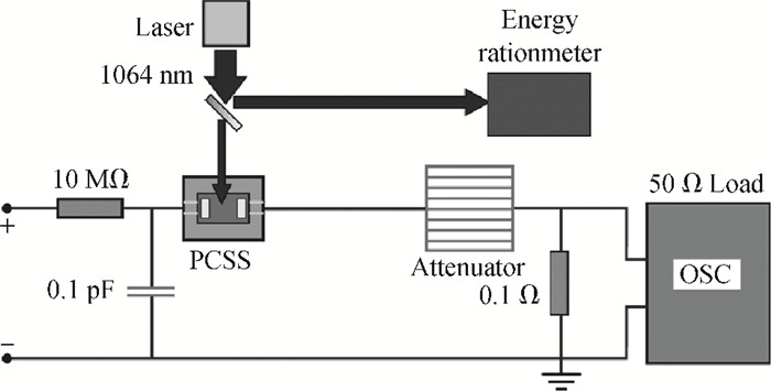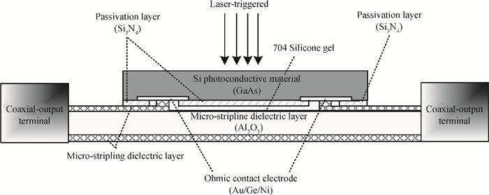
Fig. 1.
Structural diagram of SI-GaAs PCSS.
SEMICONDUCTOR DEVICES
Xiangrong Ma1, 2, , Wei Shi1 and Mei Xiang2
Corresponding author: Ma Xiangrong, Email:mxr310@163.com
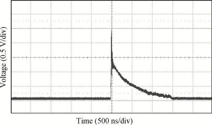
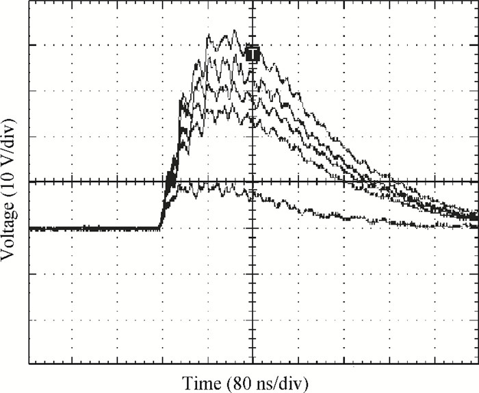
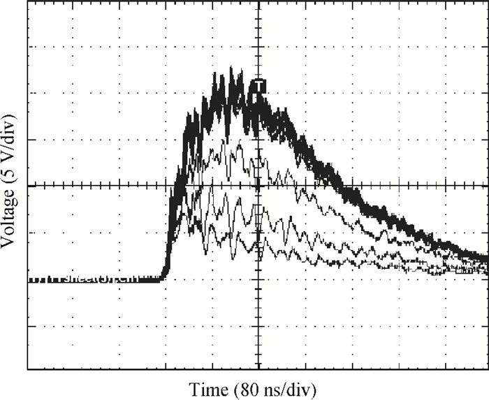
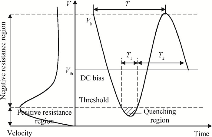
Abstract: Experiments with the limited space-charge accumulation (LSA) mode of oscillation in a large gap semi-insulating (SI) GaAs photoconductive semiconductor switch (PCSS) are discussed. It has been observed that growth and drift of a photo-activated charge domain (PACD) are quenched only when the bias voltage is more than twice the threshold voltage. The original negative resistance characteristics are directly utilized in the LSA mode; during LSA operation the spatial average of the electric field varies over a large portion of the negative differential mobility region of the velocity-electric field characteristic. The work efficiency of an SI GaAs PCSS is remarkably enhanced by electric field excursions into the positive resistance region when the total electric field is only below the threshold part of the time. The LSA mode can only operate in the certain conditions that satisfy the quenching of the accumulation layer and the smaller initial domain voltage.
Keywords: GaAs photoconductive semiconductor switch, limit space charge accumulate mode, accumulation layer, photo-activated charge domain
| [1] |
Shi Wei, Dai Huiying, Sun Xiaowei. Photon-activated charge domain in high-gain photoconductive switches. Chin Opt Lett, 2003, 1(9):553 https://www.osapublishing.org/col/abstract.cfm?uri=col-1-9-553
|
| [2] |
Shi W, Tian L. Mechanism analysis of periodicity and weakening surge of GaAs photoconductive semiconductor switches. Appl Phys Lett, 2006, 89(20):202103 doi: 10.1063/1.2387120
|
| [3] |
Shi Wei, Jia Wanli, Ji Weili. Ultra-wideband electromagnetic radiation from GaAs photoconductive switches. Chinese Journal of Semiconductors, 2005, 26(1):11 doi: 10.1002/mop.26683/pdf
|
| [4] |
Shi Wei, Jia Wanli, Hou Lei, et al. Terahertz radiation from large aperture bulk semi-insulating GaAs photoconductive dipole antenna. Chin Phys Lett, 2004, 21(9):1842 doi: 10.1088/0256-307X/21/9/047
|
| [5] |
Williamson S, Albrecht G F, Mourou M. Laser triggered Cr:GaAs HV spark gap with high sensitivity. Rev Sci Inst, 1982, 53(6):867 doi: 10.1063/1.1137071
|
| [6] |
Loubriel G M, O'Malley M W, Zutavern F J. Toward pulsed power uses for photoconductive semiconductor switches. Proceedings of the 6th IEEE International Pulsed Power Conference, Albuquerque, USA, 1987 https://www.osti.gov/scitech/biblio/6179591
|
| [7] |
Loubriel G M, Zutavern F J, O'Malley M W, et al. High gain GaAs switches for impulse sources:measurement of the speed of current filaments. IEEE Power Modulator Symposium, Washington, USA, 1994 http://ieeexplore.ieee.org/document/597058/?reload=true&arnumber=597058
|
| [8] |
Loubriel G M, Zutavern F J, Hjalmarson H P, et al. Measurement of the velocity of current filaments in optically triggered high gain GaAs switches. Appl Phys Lett, 1994, 64(6):3323 doi: 10.1063/1.111266
|
| [9] |
Zhao H, Hadizad P, Jung H, et al. Avalanche injection model for the lock-on effect in Ⅲ-Ⅴ power photoconductive switches. J Appl Phys, 1993, 73(4):1807 doi: 10.1063/1.353190
|
| [10] |
Shi W, Tian L, Liu Z, et al. 30 kV and 3 kA semi-insulating GaAs photoconductive semiconductor switch. Appl Phys Lett, 2008, 92(4):043511 doi: 10.1063/1.2838743
|
| [11] |
Shi Wei, Wang Xingmei, Hou Lei, et al. Design and performance of a high-gain double-layer GaAs photoconductive switch. Acta Physica Sinica, 2008, 57(11):7185
|
| [12] |
Copeland J A. A new mode of operation for bulk negative resistance oscillators. Proc IEEE, 1966, 54(10):1479 doi: 10.1109/PROC.1966.5158
|
| [13] |
Copeland J A. Stable space-charge layers in two-valley semiconductors. J Appl Phys, 1966, 37(9):3602 doi: 10.1063/1.1708911
|
| [14] |
Copeland J A. LSA oscillator waveforms for high efficiency. Proc IEEE, 1969, 57(9):1966 http://ieeexplore.ieee.org/document/1449288/?reload=true&arnumber=1449288&contentType=Journals%20%26%20Magazines
|
| [15] |
Curtice W R, Purcell J J. Analysis of LSA mode including effects of space charge and intervalley transfer time. IEEE Trans Electron Devices, 1970, ED-17(12):1048 http://ieeexplore.ieee.org/document/1476309/
|
| [16] |
Kuru I, Robson P N, Kino G S. Some measurements of the steady-state and transient characteristics of high-field dipole domains in GaAs. IEEE Trans Electron Devices, 1968, 15(1):21 doi: 10.1109/T-ED.1968.16131
|
| [17] |
Jones D, Rees H D. Electron-relaxation effects in transferred-electron devices revealed by new simulation method. Electron Lett, 1972, 8(14):363 doi: 10.1049/el:19720265
|
| [18] |
Jones D, Rees H D. Overlength modes of InP transferred-electron devices. Electron Lett, 1974, 10(12):234 doi: 10.1049/el:19740181
|
| [19] |
Kim K W, Kochelap V A, Woolard D L. Terahertz generation in submicron GaN diodes within the limited space-charge accumulation regime. J Appl Phys, 2005, 98(6):064507 doi: 10.1063/1.2060956
|
| [20] |
Sokolov V N, Kim K W, Trew R J. Large-signal analysis of terahertz generation in submicrometer GaN diodes. IEEE Sensors J, 2010, 10(3):765 doi: 10.1109/JSEN.2009.2038132
|
| [21] |
Wickenden A E. Efficient terahertz generation by carbon nanotubes within the limited space-charge accumulation regime. J Appl Phys, 2009, 105(9):094316 doi: 10.1063/1.3123806
|
| [22] |
Kennedy W K, Eastman L F, Gilbert R J. LSA operation of large volume bulk GaAs samples. IEEE Trans Electron Devices, 1967, 14(9):500 doi: 10.1109/T-ED.1967.15994
|
| [23] |
Olsson K O I. LSA diode theory for long samples. IEEE Trans Electron Devices, 1969, ED-16(2):202 http://ieeexplore.ieee.org/document/1475632/
|
| [24] |
Shi W, Qu G, Xu M, et al. Current limiting effects of photoactivated charge domain in semi-insulating GaAs photoconductive switch. Appl Phys Lett, 2009, 94(7):072110 doi: 10.1063/1.3086886
|
| [25] |
Ma X R, Shi W, Ji W L, et al. The overvoltage LSA relaxation mode studies in photoconductive semiconductor switch. International Symposium on Photonics and Optoelectronics, SOPO, 2010, 5504:407 http://ieeexplore.ieee.org/document/5504407/
|
| [26] |
Shi Wei, Ma Xiangrong. Peculiar transmission characteristics for the large gap semi-insulating GaAs photoconductive switch. Chin Phys Lett, 2011, 28(12):42011
|
| [27] |
Copeland J A. LSA oscillator-diode theory. J Appl Phys, 1967, 38(8):3096 doi: 10.1063/1.1710069
|


Article views: 3043 Times PDF downloads: 10 Times Cited by: 0 Times
Received: 03 December 2012 Revised: 02 January 2013 Online: Published: 01 July 2013
| Citation: |
Xiangrong Ma, Wei Shi, Mei Xiang. Experimental investigation of limit space charge accumulation mode operation in a semi-insulating GaAs photoconductive semiconductor switch[J]. Journal of Semiconductors, 2013, 34(7): 074011. doi: 10.1088/1674-4926/34/7/074011
****
X R Ma, W Shi, M Xiang. Experimental investigation of limit space charge accumulation mode operation in a semi-insulating GaAs photoconductive semiconductor switch[J]. J. Semicond., 2013, 34(7): 074011. doi: 10.1088/1674-4926/34/7/074011.

|
| [1] |
Shi Wei, Dai Huiying, Sun Xiaowei. Photon-activated charge domain in high-gain photoconductive switches. Chin Opt Lett, 2003, 1(9):553 https://www.osapublishing.org/col/abstract.cfm?uri=col-1-9-553
|
| [2] |
Shi W, Tian L. Mechanism analysis of periodicity and weakening surge of GaAs photoconductive semiconductor switches. Appl Phys Lett, 2006, 89(20):202103 doi: 10.1063/1.2387120
|
| [3] |
Shi Wei, Jia Wanli, Ji Weili. Ultra-wideband electromagnetic radiation from GaAs photoconductive switches. Chinese Journal of Semiconductors, 2005, 26(1):11 doi: 10.1002/mop.26683/pdf
|
| [4] |
Shi Wei, Jia Wanli, Hou Lei, et al. Terahertz radiation from large aperture bulk semi-insulating GaAs photoconductive dipole antenna. Chin Phys Lett, 2004, 21(9):1842 doi: 10.1088/0256-307X/21/9/047
|
| [5] |
Williamson S, Albrecht G F, Mourou M. Laser triggered Cr:GaAs HV spark gap with high sensitivity. Rev Sci Inst, 1982, 53(6):867 doi: 10.1063/1.1137071
|
| [6] |
Loubriel G M, O'Malley M W, Zutavern F J. Toward pulsed power uses for photoconductive semiconductor switches. Proceedings of the 6th IEEE International Pulsed Power Conference, Albuquerque, USA, 1987 https://www.osti.gov/scitech/biblio/6179591
|
| [7] |
Loubriel G M, Zutavern F J, O'Malley M W, et al. High gain GaAs switches for impulse sources:measurement of the speed of current filaments. IEEE Power Modulator Symposium, Washington, USA, 1994 http://ieeexplore.ieee.org/document/597058/?reload=true&arnumber=597058
|
| [8] |
Loubriel G M, Zutavern F J, Hjalmarson H P, et al. Measurement of the velocity of current filaments in optically triggered high gain GaAs switches. Appl Phys Lett, 1994, 64(6):3323 doi: 10.1063/1.111266
|
| [9] |
Zhao H, Hadizad P, Jung H, et al. Avalanche injection model for the lock-on effect in Ⅲ-Ⅴ power photoconductive switches. J Appl Phys, 1993, 73(4):1807 doi: 10.1063/1.353190
|
| [10] |
Shi W, Tian L, Liu Z, et al. 30 kV and 3 kA semi-insulating GaAs photoconductive semiconductor switch. Appl Phys Lett, 2008, 92(4):043511 doi: 10.1063/1.2838743
|
| [11] |
Shi Wei, Wang Xingmei, Hou Lei, et al. Design and performance of a high-gain double-layer GaAs photoconductive switch. Acta Physica Sinica, 2008, 57(11):7185
|
| [12] |
Copeland J A. A new mode of operation for bulk negative resistance oscillators. Proc IEEE, 1966, 54(10):1479 doi: 10.1109/PROC.1966.5158
|
| [13] |
Copeland J A. Stable space-charge layers in two-valley semiconductors. J Appl Phys, 1966, 37(9):3602 doi: 10.1063/1.1708911
|
| [14] |
Copeland J A. LSA oscillator waveforms for high efficiency. Proc IEEE, 1969, 57(9):1966 http://ieeexplore.ieee.org/document/1449288/?reload=true&arnumber=1449288&contentType=Journals%20%26%20Magazines
|
| [15] |
Curtice W R, Purcell J J. Analysis of LSA mode including effects of space charge and intervalley transfer time. IEEE Trans Electron Devices, 1970, ED-17(12):1048 http://ieeexplore.ieee.org/document/1476309/
|
| [16] |
Kuru I, Robson P N, Kino G S. Some measurements of the steady-state and transient characteristics of high-field dipole domains in GaAs. IEEE Trans Electron Devices, 1968, 15(1):21 doi: 10.1109/T-ED.1968.16131
|
| [17] |
Jones D, Rees H D. Electron-relaxation effects in transferred-electron devices revealed by new simulation method. Electron Lett, 1972, 8(14):363 doi: 10.1049/el:19720265
|
| [18] |
Jones D, Rees H D. Overlength modes of InP transferred-electron devices. Electron Lett, 1974, 10(12):234 doi: 10.1049/el:19740181
|
| [19] |
Kim K W, Kochelap V A, Woolard D L. Terahertz generation in submicron GaN diodes within the limited space-charge accumulation regime. J Appl Phys, 2005, 98(6):064507 doi: 10.1063/1.2060956
|
| [20] |
Sokolov V N, Kim K W, Trew R J. Large-signal analysis of terahertz generation in submicrometer GaN diodes. IEEE Sensors J, 2010, 10(3):765 doi: 10.1109/JSEN.2009.2038132
|
| [21] |
Wickenden A E. Efficient terahertz generation by carbon nanotubes within the limited space-charge accumulation regime. J Appl Phys, 2009, 105(9):094316 doi: 10.1063/1.3123806
|
| [22] |
Kennedy W K, Eastman L F, Gilbert R J. LSA operation of large volume bulk GaAs samples. IEEE Trans Electron Devices, 1967, 14(9):500 doi: 10.1109/T-ED.1967.15994
|
| [23] |
Olsson K O I. LSA diode theory for long samples. IEEE Trans Electron Devices, 1969, ED-16(2):202 http://ieeexplore.ieee.org/document/1475632/
|
| [24] |
Shi W, Qu G, Xu M, et al. Current limiting effects of photoactivated charge domain in semi-insulating GaAs photoconductive switch. Appl Phys Lett, 2009, 94(7):072110 doi: 10.1063/1.3086886
|
| [25] |
Ma X R, Shi W, Ji W L, et al. The overvoltage LSA relaxation mode studies in photoconductive semiconductor switch. International Symposium on Photonics and Optoelectronics, SOPO, 2010, 5504:407 http://ieeexplore.ieee.org/document/5504407/
|
| [26] |
Shi Wei, Ma Xiangrong. Peculiar transmission characteristics for the large gap semi-insulating GaAs photoconductive switch. Chin Phys Lett, 2011, 28(12):42011
|
| [27] |
Copeland J A. LSA oscillator-diode theory. J Appl Phys, 1967, 38(8):3096 doi: 10.1063/1.1710069
|

 WeChat ID
Journal of Semiconductors © 2017 All Rights Reserved 京ICP备05085259号-2

 DownLoad: