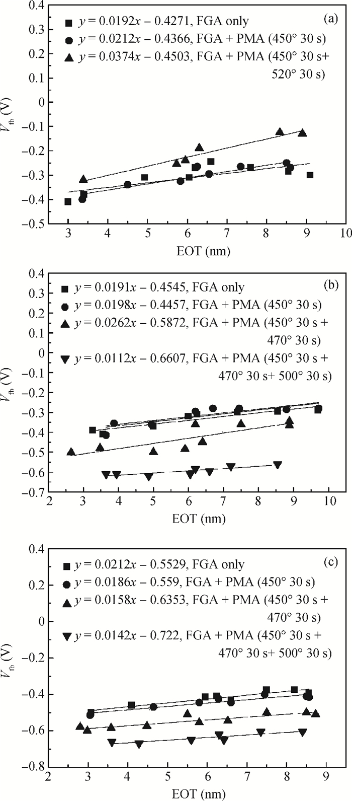
Processing math: 100%
J. Semicond. > 2013, Volume 34 > Issue 7 > 076003

SEMICONDUCTOR TECHNOLOGY

Modulation of the effective work function of a TiN metal gate for NMOS requisition with Al incorporation

Kai Han, Xueli Ma, Hong Yang and Wenwu Wang

+ Author Affiliations

 Corresponding author: Han Kai, hankai@ime.ac.cn

DOI: 10.1088/1674-4926/34/7/076003

PDF

Abstract: The effect of Al incorporation on the effective work function (EWF) of TiN metal gate was systematically investigated. Metal-oxide-semiconductor (MOS) capacitors with W/TiN/Al/TiN gate stacks were used to fulfill this purpose. Different thickness ratios of Al to TiN and different post metal annealing (PMA) conditions were employed. Significant shift of work function towards to Si conduction band was observed, which was suitable for NMOS and the magnitude of shift depends on the processing conditions.

Key words: work function modulationAlMOS capacitorPMA

The continuous scaling of metal-oxide-semiconductor (MOS) transistors makes it imperative to replace the conventional SiO2/poly-Si structure with high-k dielectric/metal gate stack[1-3]. The integration of high-k dielectric/metal gate stack into MOS transistor, however, faces challenges such as threshold voltage (Vth) control. Generally, band edge metal gates are needed to obtain low Vth for bulk CMOS application[4]. Among all the potential candidates for metal gate, TiN is widely studied because of its superior performance such as stability when contacted with high-k dielectrics, low resistivity, and process compatibility[5, 6]. However, the EWF of TiN lies at the mid-gap of silicon or beyond. Modulating the EWF of a TiN metal gate to meet the NMOS requirement is of interest, and Al incorporation is considered promising[7]. However, for gate-last integration scheme, a low thermal budget is necessary. So finding appropriate Al incorporation conditions suitable for gate-last integration is important. In this work, capacitors with W/TiN/Al/TiN gate stacks were fabricated to investigate the effect of Al incorporation and low temperature annealing on the EWF of TiN.

Firstly, 10 nm SiO2 films were thermally grown on diluted-HF last P type Si wafers (1.34 × 1015 cm-3), and then the thick SiO2 films were wet etched to have a terraced structure. Then two sets of samples were fabricated with W 100 nm/TiN 15 nm/Al 5 nm/TiN 10 nm and W 100 nm/TiN 20 nm/Al 5 nm/TiN 5 nm stacks deposited on the terraced SiO2 in-situ in ULVAC-2306, respectively. A control sample with W 100 nm/TiN 30 nm was also prepared. Then, after back oxide removal, Al metallization and forming gas annealing (FGA) (380 ℃, 20 min, NO2 : HO2 = 10 : 1) were performed. And then all samples underwent various annealing conditions, which are collectively named as post-metal annealing (PMA) in the present work. PMA was performed in NO2 ambience at atmosphere pressure. Furthermore, capacitors with atomic layer deposited (ALD) HfO2 dielectrics were also fabricated to confirm the effect of Al incorporation on the EWF of, TiN. 2.97 nm thick HfO2 films, whose thickness was calibrated from the X-ray reflection spectrum, were deposited on the diluted-HF last P type Si wafers using TEMAHf as precursor and HO2O as oxidant respectively, which was finished at 300 ℃ in TFS200. And metal gate conditions will be discussed in detail in the subsequent section. The C-V characteristics of the capacitors were measured at a frequency of 1 MHz with MDC 7200 and fitted with QMCV model.

For capacitors with a terraced SiO2 structure, the relationship of flat band voltage (Vfb) versus equivalent oxide thickness (EOT) is expressed by

Vfb=ϕmsQSiO2,SiEOT/ε0εSiO2,
(1)

where ϕms is the work function difference between the metal gate (ϕm) and Si substrate (ϕs). QSiO2, Si is the areal charge densities (per unit area) at SiO2/Si interface. ε0 and ε SiO2 express the vacuum permittivity and the relative permittivity of SiO2, respectively. The EWF of the metal gate can be obtained from ϕ s plus ϕ ms. The work function of Si substrate (ϕs) in this work is calculated to be 4.91 eV.

Vfb-EOT curves for samples with terraced SiO2 structures which undergo FGA only are shown in Fig. 1. As shown in Fig. 1, the EWF of TiN metal gate without Al incorporation is 4.48 eV. The EWF of metal gates with Al incorporation are 4.46 eV and 4.36 eV for samples with 10 nm bottom TiN and 5 nm bottom TiN respectively. The sample with 5 nm bottom TiN shows more negative ϕ ms shift while the sample with 10 nm bottom TiN shows tiny ϕ ms shift. The phenomenon is in good agreement with our previous work that only about 10 nm thickness of metal gate on a high-k dielectric plays the role as work function layer. It is obvious that a bottom TiN layer with 10 nm is thick enough to screen the effect of Al on the work function. However, the result of the sample with 5 nm bottom TiN shows the competence of Al to modulate the work function of TiN metal gate because of its lower work function. So it is important to select an appropriate bottom TiN thickness for the application of Al incorporation.

Figure  1.  Vfb versus EOT curves for samples with and w/o Al incorporation on terraced-SiO2 undergoing FGA only.

It is considered that PMA can affect the modulating ability of Al. This is because PMA is an effective method to drive the Al downward, which further affects the work function of TiN metal gate. So different PMA conditions are imposed on all samples to investigate the effect of PMA on the EWF of metal gates. The results are shown in Fig. 2. Figure 2(a) shows the Vfb-EOT relationships of a sample without Al. As shown in Fig. 2(a), the ϕ ms shows a slight shift due to thermal annealing which testifies the good thermal stability of the TiN metal gate. The Vfb-EOT relationships of the sample with 5 nm Al and 10 nm bottom TiN are shown in Fig. 2(b). As shown in Fig. 2(b), when the sample is annealed at 450 ℃ for 30 s, the ϕ ms is almost the same as that without PMA. However, when additional annealing at 470 ℃ for 30 s is exerted, the ϕ ms significantly shifts by as much as 130 meV and the ϕ ms is further decreased by another annealing at 500 ℃ for 30 s. After the total annealing, the ϕ ms negatively shifts by as much as 210 meV, and the EWF of the metal gate is 4.25 eV. Figure 2(c) shows the Vfb-EOT relationships of the sample with Al and 5 nm bottom TiN. From Fig. 2(c), the same tendency of ϕ ms shift is observed. And the EWF of the metal gate is 4.19 eV, which is lower than the sample with a 10 nm bottom TiN layer. Also from Figs. 2(b) and 2(c), it can be found that there is a threshold of PMA to make the Al diffuse.

Figure  2.  Vfb versus EOT curves for samples (a) w/o Al incorporation, (b) 5 nm Al with 10 nm bottom TiN, (c) 5 nm Al with 5 nm bottom TiN undergoing FGA and different PMA conditions.

From the discussion above, we can conclude that Al incorporation is an effective approach to modulate the EWF of TiN metal gate; higher PMA temperature makes more negative shift and a thicker bottom TiN layer blocks the diffusion of Al. The crux of Al incorporation is to select an appropriate Al/TiN ratio and PMA condition. In order to confirm the effect of Al incorporation on the EWF of a TiN metal gate when the EOT is below 1 nm and provide practicable conditions for NMOS, capacitors with 2.97 nm ALD-HfO2 were fabricated and the EOT of all samples are fitted to be less than 1 nm. And Vfb is employed to indicate the effect of Al incorporation on the EWF of a metal gate.

Figure 3 shows the C-V plots of the samples with W 100 nm/TiN 20 nm/Al 5 nm/TiN 5 nm/ALD-HfO2 2.97 nm/Si structure undergoing different PMA conditions. The C-V curve of the sample without Al with FGA only is also shown as reference. As shown in Fig. 3, the EOT of all samples are below 1 nm. And also as shown in Fig. 3, the negative shift of Vfb can be observed as much as 270 mV, which confirm the EWF modulating competence of Al incorporation. But we can also see from the plot that there is a critical temperature, if the thermal process is higher than it, the ϕ ms will shift positively. This may result from the Al diffusing into the HfO2 film and forming the dipole at HfO2/SiO2 interface. And another notable point is that the threshold of driving Al diffusing is lower than that discussed above. The effect of HfO2 can be excluded because the Vfb of sample with W/TiN/HfO2 structure shows no response to PMA up to 470 ℃ according to our previous work. And we can find that the work function of TiN metal gate here is about 4.7 eV which is higher than that used above. The difference of TiN layer may result in different diffusivity of Al. Also as shown in Fig. 3, EOT decreases as PMA temperature increases which is attributed to oxygen scavenging due to Al incorporation.

Figure  3.  CV plots of the sample with W/TiN/5 nmAl/5 nmTiN/ALDHfO2/Si structure undergoing different PMA conditions.

In order to select an optimized condition more suitable for NMOS. The thickness of the bottom TiN layer is further decreased. A capacitor with W 100 nm/TiN 23 nm/Al 4 nm/TiN 3 nm/ALD-HfO2 2.97 nm gate stack was fabricated. Figure 4 shows the C-V plots of the samples. By appropriate annealing, as much as 410 mV Vfb shift can be obtained, which is more suitable for NMOS. And positive shift of Vfb can also be seen from Fig. 4 when annealed at 370 ℃ for 60 s.

Figure  4.  CV plots of the sample with W/TiN/4 nm Al/3 nm TiN/ALDHfO2/Si structure undergoing different PMA conditions.

It is important to confirm the feasibility of EWF modulation by Al incorporation from the viewpoint of CMOS integration. In order to achieve this purpose, a sample with annealing suitable for PMOS was fabricated. The detailed process flow is as follows: after 2.97 nm HfO2 deposition on the HF-last substrate, post deposition annealing (PDA) at 470 ℃ for 15 s at NO2 with traces of O2 ambience was performed. And then 3 nm TiN was deposited followed by 450 ℃ 60 s annealing with the same ambience as PDA. Such annealing can make Vfb positive shift which is more suitable for PMOS (not shown here). Then W 100 nm/TiN 23 nm/Al 4 nm was capped. Backside metallization and FGA (380, 20 min, NO2 : HO2 = 10 : 1) were also imposed. Figure 5 shows the C-V plots of the sample with different PMA conditions. Significant Vfb shift prove the feasibility of EWF modulation by Al incorporation. And compared with the sample without PDA and PMA, the enhanced effect of Al on work function can also be observed. When annealed at 370 ℃ for 30 s, the Vfb shift of the sample with PDA and PMA is 380 meV, while that for the sample without PDA and PMA is 120 meV. And PMA can change the work function of a TiN metal gate. This further proves the supposition that a different TiN layer may result in different diffusivity of Al.

Figure  5.  CV plots of the sample with W/TiN/4 nm Al/3 nm TiN/ALDHfO2/Si structure undergoing annealing suitable for PMOS and different PMA conditions.

We have systematically studied the impact of Al incorporation on the EWF of a TiN metal gate with terraced-SiO2 and ALD-HfO2 as dielectrics respectively, and find that Al incorporation makes the EWF of TiN shift toward the conduction band of Si significantly. The Al/TiN thickness ratio and PMA conditions have a significant influence on the work function modulation of Al incorporation. Appropriate conditions are given in present work which can be used in NMOS devices.


[1]
Wilk G D, Wallace R M, Anthony J M. High-k gate dielectrics:current status and materials properties considerations. J Appl Phys, 2001, 89(10):5243
[2]
Zhao Y, Masahiro T, Koji K, et al. Moisture-absorption-induced permittivity deterioration and surface roughness enhancement of lanthanum oxide films on silicon. Appl Phys Lett, 2006, 88(7):072904 doi: 10.1063/1.2174840
[3]
Chau R, Brask J, Datta S, et al. Application of high-k gate dielectrics and metal gate electrodes to enable silicon and non-silicon logic nanotechnology. Microelectron Eng, 2005, 80:1 doi: 10.1016/j.mee.2005.04.035
[4]
Narayanan V, Paruchuri V K, Bojarczuk N A, et al. Band-edge high-performance high-k/metal gate n-MOSFETs using cap layers containing group ⅡA and ⅢB elements with gate-first processing for 45 nm and beyond. Dig Tech Pap Symp VLSI Technol, 2006:224
[5]
Masaru K, Takeo M, Seiichi M, et al. Effective-work-function control by varying the TiN thickness in poly-Si/TiN gate electrodes for scaled high-k CMOSFETs. IEEE Electron Device Lett, 2009, 30(5):466 doi: 10.1109/LED.2009.2016585
[6]
Jörgen W, Gustaf S, Jörgen O. Variable work function in MOS capacitors utilizing nitrogen-controlled TiNx gate electrodes. Microelectron Eng, 2004, 75:389 doi: 10.1016/j.mee.2004.07.061
[7]
Wang Xiaorong, Jiang Yulong, Xie Qi. Annealing effect on the metal gate effective work function modulation for the Al/TiN/SiO2/p-Si structure. Microelectron Eng, 2011, 88:573 doi: 10.1016/j.mee.2010.06.029
Fig. 1.  Vfb versus EOT curves for samples with and w/o Al incorporation on terraced-SiO2 undergoing FGA only.

Fig. 2.  Vfb versus EOT curves for samples (a) w/o Al incorporation, (b) 5 nm Al with 10 nm bottom TiN, (c) 5 nm Al with 5 nm bottom TiN undergoing FGA and different PMA conditions.

Fig. 3.  CV plots of the sample with W/TiN/5 nmAl/5 nmTiN/ALDHfO2/Si structure undergoing different PMA conditions.

Fig. 4.  CV plots of the sample with W/TiN/4 nm Al/3 nm TiN/ALDHfO2/Si structure undergoing different PMA conditions.

Fig. 5.  CV plots of the sample with W/TiN/4 nm Al/3 nm TiN/ALDHfO2/Si structure undergoing annealing suitable for PMOS and different PMA conditions.

[1]
Wilk G D, Wallace R M, Anthony J M. High-k gate dielectrics:current status and materials properties considerations. J Appl Phys, 2001, 89(10):5243
[2]
Zhao Y, Masahiro T, Koji K, et al. Moisture-absorption-induced permittivity deterioration and surface roughness enhancement of lanthanum oxide films on silicon. Appl Phys Lett, 2006, 88(7):072904 doi: 10.1063/1.2174840
[3]
Chau R, Brask J, Datta S, et al. Application of high-k gate dielectrics and metal gate electrodes to enable silicon and non-silicon logic nanotechnology. Microelectron Eng, 2005, 80:1 doi: 10.1016/j.mee.2005.04.035
[4]
Narayanan V, Paruchuri V K, Bojarczuk N A, et al. Band-edge high-performance high-k/metal gate n-MOSFETs using cap layers containing group ⅡA and ⅢB elements with gate-first processing for 45 nm and beyond. Dig Tech Pap Symp VLSI Technol, 2006:224
[5]
Masaru K, Takeo M, Seiichi M, et al. Effective-work-function control by varying the TiN thickness in poly-Si/TiN gate electrodes for scaled high-k CMOSFETs. IEEE Electron Device Lett, 2009, 30(5):466 doi: 10.1109/LED.2009.2016585
[6]
Jörgen W, Gustaf S, Jörgen O. Variable work function in MOS capacitors utilizing nitrogen-controlled TiNx gate electrodes. Microelectron Eng, 2004, 75:389 doi: 10.1016/j.mee.2004.07.061
[7]
Wang Xiaorong, Jiang Yulong, Xie Qi. Annealing effect on the metal gate effective work function modulation for the Al/TiN/SiO2/p-Si structure. Microelectron Eng, 2011, 88:573 doi: 10.1016/j.mee.2010.06.029
1

Perovskite plasmonic lasers capable of mode modulation

Jingbi You

Journal of Semiconductors, 2019, 40(7): 070203. doi: 10.1088/1674-4926/40/7/070203

2

Analytical model for the effects of the variation of ferrolectric material parameters on the minimum subthreshold swing in negative capacitance capacitor

Raheela Rasool, Najeeb-ud-Din, G. M. Rather

Journal of Semiconductors, 2019, 40(12): 122401. doi: 10.1088/1674-4926/40/12/122401

3

Improved interfacial properties of GaAs MOS capacitor with NH3-plasma-treated ZnON as interfacial passivation layer

Jingkang Gong, Jingping Xu, Lu Liu, Hanhan Lu, Xiaoyu Liu, et al.

Journal of Semiconductors, 2017, 38(9): 094004. doi: 10.1088/1674-4926/38/9/094004

4

The effect of nitridation and sulfur passivation for In0.53Ga0.47As surfaces on their Al/Al2O3/InGaAs MOS capacitors properties

Zizeng Lin, Mingmin Cao, Shengkai Wang, Qi Li, Gongli Xiao, et al.

Journal of Semiconductors, 2016, 37(2): 026002. doi: 10.1088/1674-4926/37/2/026002

5

Theoretical study of defect impact on two-dimensional MoS2

Anna V. Krivosheeva, Victor L. Shaposhnikov, Victor E. Borisenko, Jean-Louis Lazzari, Chow Waileong, et al.

Journal of Semiconductors, 2015, 36(12): 122002. doi: 10.1088/1674-4926/36/12/122002

6

VCCS controlled LDO with small on-chip capacitor

Qiuli Li, Yao Qian, Danzhu Lü, Zhiliang Hong

Journal of Semiconductors, 2014, 35(11): 115011. doi: 10.1088/1674-4926/35/11/115011

7

Modulation of the effective work function of TiN metal gate for PMOS application

Kai Han, Xueli Ma, Hong Yang, Wenwu Wang

Journal of Semiconductors, 2013, 34(8): 086002. doi: 10.1088/1674-4926/34/8/086002

8

Low-power switched-capacitor delta-sigma modulator for EEG recording applications

Chen Jin, Zhang Xu, Chen Hongda

Journal of Semiconductors, 2010, 31(7): 075009. doi: 10.1088/1674-4926/31/7/075009

9

Conductivity modulation enhanced lateral IGBT with SiO2 shielded layer anode by SIMOX technology on SOI substrate

Chen Wensuo, Zhang Bo, Li Zhaoji, Fang Jian, Guan Xu, et al.

Journal of Semiconductors, 2010, 31(6): 064004. doi: 10.1088/1674-4926/31/6/064004

10

A low-power and low-phase-noise LC digitally controlled oscillator featuring a novel capacitor bank

Tian Huanhuan, Li Zhiqiang, Chen Pufeng, Wu Rufei, Zhang Haiying, et al.

Journal of Semiconductors, 2010, 31(12): 125003. doi: 10.1088/1674-4926/31/12/125003

11

Comparison of electron transmittances and tunneling currents in an anisotropic TiNx/HfO2/SiO2/p-Si(100) metal–oxide–semiconductor (MOS) capacitor calculated using exponential- and Airy-wavefunction app

Fatimah A. Noor, Mikrajuddin Abdullah, Sukirno, Khairurrijal

Journal of Semiconductors, 2010, 31(12): 124002. doi: 10.1088/1674-4926/31/12/124002

12

Memory characteristics of an MOS capacitor structure with double-layer semiconductor and metal heterogeneous nanocrystals

Ni Henan, Wu Liangcai, Song Zhitang, Hui Chun

Journal of Semiconductors, 2009, 30(11): 114003. doi: 10.1088/1674-4926/30/11/114003

13

TDDB improvement by optimized processes on metal–insulator–silicon capacitors with atomic layer deposition of Al2O3 and multi layers of TiN film structure

Peng Kun, Wang Biao, Xiao Deyuan, Qiu Shengfen, Lin D C, et al.

Journal of Semiconductors, 2009, 30(8): 082005. doi: 10.1088/1674-4926/30/8/082005

14

A capacitor-free CMOS LDO regulator with AC-boosting and active-feedback frequency compensation

Zhou Qianneng, Wang Yongsheng, Lai Fengchang

Journal of Semiconductors, 2009, 30(4): 045006. doi: 10.1088/1674-4926/30/4/045006

15

Capacitance–voltage characterization of fully silicided gated MOS capacitor

Wang Baomin, Ru Guoping, Jiang Yulong, Qu Xinping, Li Bingzong, et al.

Journal of Semiconductors, 2009, 30(3): 034002. doi: 10.1088/1674-4926/30/3/034002

16

A Capacitor-Free CMOS Low-Dropout Regulator for System-on-Chip Application

Han Peng, Wang Zhigong, Xu Yong, Li Wei

Journal of Semiconductors, 2008, 29(8): 1507-1510.

17

Dual-Work-Function Ni-FUSI Metal Gate for CMOS Technology

Zhou Huajie, Xu Qiuxia

Chinese Journal of Semiconductors , 2007, 28(10): 1532-1539.

18

Parameter Extraction for 2-π Equivalent Circuit Modelof RF CMOS Spiral Inductors

Gao Wei, Yu Zhiping

Chinese Journal of Semiconductors , 2006, 27(4): 667-673.

19

An Optoelectronic Pulse Frequency Modulation Circuitfor Retinal Prosthesis

Liu Jinbin, Chen Hongda, Gao Peng, Pei Weihua, Sui Xiaohong, et al.

Chinese Journal of Semiconductors , 2006, 27(4): 700-704.

20

Electrical Characteristics of n-Type 4H-SiC MOS Capacitor

Ning Jin, Liu Zhongli, Gao Jiantou

Chinese Journal of Semiconductors , 2005, 26(S1): 140-142.

  • Search

    Advanced Search >>

    GET CITATION

    Kai Han, Xueli Ma, Hong Yang, Wenwu Wang. Modulation of the effective work function of a TiN metal gate for NMOS requisition with Al incorporation[J]. Journal of Semiconductors, 2013, 34(7): 076003. doi: 10.1088/1674-4926/34/7/076003
    K Han, X L Ma, H Yang, W W Wang. Modulation of the effective work function of a TiN metal gate for NMOS requisition with Al incorporation[J]. J. Semicond., 2013, 34(7): 076003. doi: 10.1088/1674-4926/34/7/076003.
    shu

    Export: BibTex EndNote

    Article Metrics

    Article views: 3660 Times PDF downloads: 146 Times Cited by: 0 Times

    History

    Received: 23 October 2012 Revised: 13 February 2013 Online: Published: 01 July 2013

    Catalog

      Email This Article

      User name:
      Email:*请输入正确邮箱
      Code:*验证码错误
      Kai Han, Xueli Ma, Hong Yang, Wenwu Wang. Modulation of the effective work function of a TiN metal gate for NMOS requisition with Al incorporation[J]. Journal of Semiconductors, 2013, 34(7): 076003. doi: 10.1088/1674-4926/34/7/076003 ****K Han, X L Ma, H Yang, W W Wang. Modulation of the effective work function of a TiN metal gate for NMOS requisition with Al incorporation[J]. J. Semicond., 2013, 34(7): 076003. doi: 10.1088/1674-4926/34/7/076003.
      Citation:
      Kai Han, Xueli Ma, Hong Yang, Wenwu Wang. Modulation of the effective work function of a TiN metal gate for NMOS requisition with Al incorporation[J]. Journal of Semiconductors, 2013, 34(7): 076003. doi: 10.1088/1674-4926/34/7/076003 ****
      K Han, X L Ma, H Yang, W W Wang. Modulation of the effective work function of a TiN metal gate for NMOS requisition with Al incorporation[J]. J. Semicond., 2013, 34(7): 076003. doi: 10.1088/1674-4926/34/7/076003.

      Modulation of the effective work function of a TiN metal gate for NMOS requisition with Al incorporation

      DOI: 10.1088/1674-4926/34/7/076003
      Funds:

      the Important National Science & Technology Specific Projects of China 2009ZX02035

      the National Natural Science Foundation of China 61176091

      Project supported by the Important National Science & Technology Specific Projects of China (No. 2009ZX02035) and the National Natural Science Foundation of China (Nos. 61176091, 50932001)

      the National Natural Science Foundation of China 50932001

      More Information
      • Corresponding author: Han Kai, hankai@ime.ac.cn
      • Received Date: 2012-10-23
      • Revised Date: 2013-02-13
      • Published Date: 2013-07-01

      Catalog

        /

        DownLoad:  Full-Size Img  PowerPoint
        Return
        Return