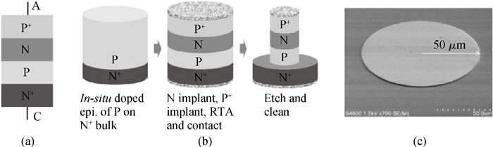
Fig. 1.
(a) Schematic of the proposed DRAM memory cell. (b) SEM view of the fabricated cell. (c) The fabrication process flow on the standard CMOS line.
SEMICONDUCTOR DEVICES
Xiaodong Tong, Hao Wu, Lichuan Zhao, Ming Wang and Huicai Zhong
Corresponding author: Tong Xiaodong, Email:tongxiaodong@ime.ac.cn
Abstract: A two-port capacitorless PNPN device with high density, high speed and low power memory fabricated using standard CMOS technology is presented. Experiments and calibrated simulations were conducted which prove that this new memory cell has a high operation speed (ns level), large read current margin (read current ratio of 104×), low process variation, good thermal reliability and available retention time (190 ms). Furthermore, the new memory cell is free of the cyclic endurance/reliability problems induced by hot-carrier injection due to the gateless structure.
Keywords: PNPN diode, two-port, cross-point
| [1] |
Ban I, Avci U E, Kencke D L, et al. A scaled floating body cell (FBC) memory with high-k + metal gate on thin-silicon and thin-BOX for 16-nm technology node and beyond. Symposium on VLSI Technology, 2008:92 http://ieeexplore.ieee.org/document/4588575/
|
| [2] |
Cho H J, Nemati F, Roy R, et al. A novel capacitor-less DRAM cell using thin capacitively-coupled thyristor (TCCT). IEEE International Electron Devices Meeting (IEDM), 2005 http://ieeexplore.ieee.org/abstract/document/1609337
|
| [3] |
Han J W, Choi Y K. Bistable resistor (biristor)-gateless silicon nanowire memory. Symposium on VLSI Technology, 2010:171 http://ieeexplore.ieee.org/document/5556215/?arnumber=5556215&filter%3DAND(p_IS_Number:5556114)%26pageNumber%3D3
|
| [4] |
Gibbons J F. A critique of the theory of p-n-p-n devices. IEEE Trans Electron Devices, 1964, 11(9):406 doi: 10.1109/T-ED.1964.15352
|
| [5] |
Kau D C, Tang S, Karpov I V, et al. A stackable cross point phase change memory. IEEE International Electron Devices Meeting (IEDM), 2009 https://www.infona.pl/resource/bwmeta1.element.ieee-art-000005424263
|
| [6] |
Tong X, Wu H, Liang Q, et al. On the design of 2-port SRAM memory cells using PNPN diodes for VLSI application. IEEE International Conference on Simulation of Semiconductor Processes and devices (SISPAD), Denver, CO, USA, 2012 doi: 10.1088/1674-4926/34/8/084005
|
| [7] |
Liang J, Jeyasingh R G D, Chen H Y, et al. An ultra-low reset current cross-point phase change memory with carbon nanotube electrodes. IEEE Trans Electron Devices, 2012, 59(4):1155 doi: 10.1109/TED.2012.2184542
|
| [8] |
Ielmini D. Modeling the universal set/reset characteristics of bipolar RRAM by field-and temperature driven filament growth. IEEE Trans Electron Devices, 1980, 27(5):939 doi: 10.1109/T-ED.1980.19960
|
| [9] |
Zhao Qiang, Zhou Maoxiu, Zhang Wei, et al. Effects of interaction between defects on the uniformity of doping HfO2-based RRAM:a first principle study. Journal of Semiconductors, 2013, 34(3):032001 doi: 10.1088/1674-4926/34/3/032001
|
| [10] |
Fu Cong, Song Zhitang, Chen Houpeng, et al. A novel low ripple charge pump with a 2X/1.5X booster for PCM. Journal of Semiconductors, 2012, 33(9):095001 doi: 10.1088/1674-4926/33/9/095001
|
| [11] |
TCAD Sentaurus User Manual. Synopsys Inc, 2010. 12
|
| [12] |
Srinivasaiah H C, Bhat N. Mixed-mode simulation approach to characterize the circuit delay sensitivity to implant dose variations. IEEE Trans Computer-Aided Design of Integrated Circuits and Systems, 2003, 22(6):742 doi: 10.1109/TCAD.2003.811453
|
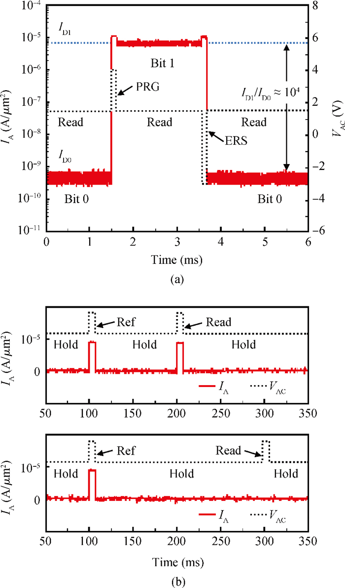
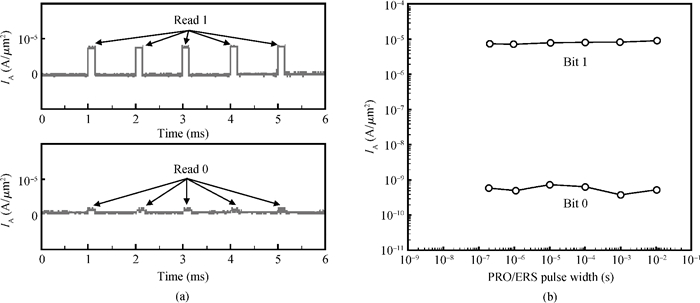
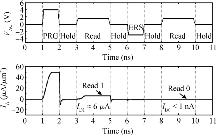
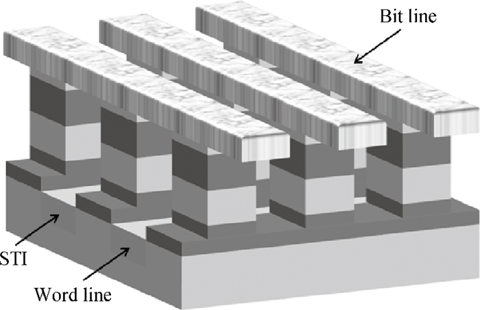
Table 1. Main performance comparisons between the biristor and the memory cell proposed in this work. The new memory cell shows much lower operation power consumption due to the different physical mechanisms from the biristor.

|
| [1] |
Ban I, Avci U E, Kencke D L, et al. A scaled floating body cell (FBC) memory with high-k + metal gate on thin-silicon and thin-BOX for 16-nm technology node and beyond. Symposium on VLSI Technology, 2008:92 http://ieeexplore.ieee.org/document/4588575/
|
| [2] |
Cho H J, Nemati F, Roy R, et al. A novel capacitor-less DRAM cell using thin capacitively-coupled thyristor (TCCT). IEEE International Electron Devices Meeting (IEDM), 2005 http://ieeexplore.ieee.org/abstract/document/1609337
|
| [3] |
Han J W, Choi Y K. Bistable resistor (biristor)-gateless silicon nanowire memory. Symposium on VLSI Technology, 2010:171 http://ieeexplore.ieee.org/document/5556215/?arnumber=5556215&filter%3DAND(p_IS_Number:5556114)%26pageNumber%3D3
|
| [4] |
Gibbons J F. A critique of the theory of p-n-p-n devices. IEEE Trans Electron Devices, 1964, 11(9):406 doi: 10.1109/T-ED.1964.15352
|
| [5] |
Kau D C, Tang S, Karpov I V, et al. A stackable cross point phase change memory. IEEE International Electron Devices Meeting (IEDM), 2009 https://www.infona.pl/resource/bwmeta1.element.ieee-art-000005424263
|
| [6] |
Tong X, Wu H, Liang Q, et al. On the design of 2-port SRAM memory cells using PNPN diodes for VLSI application. IEEE International Conference on Simulation of Semiconductor Processes and devices (SISPAD), Denver, CO, USA, 2012 doi: 10.1088/1674-4926/34/8/084005
|
| [7] |
Liang J, Jeyasingh R G D, Chen H Y, et al. An ultra-low reset current cross-point phase change memory with carbon nanotube electrodes. IEEE Trans Electron Devices, 2012, 59(4):1155 doi: 10.1109/TED.2012.2184542
|
| [8] |
Ielmini D. Modeling the universal set/reset characteristics of bipolar RRAM by field-and temperature driven filament growth. IEEE Trans Electron Devices, 1980, 27(5):939 doi: 10.1109/T-ED.1980.19960
|
| [9] |
Zhao Qiang, Zhou Maoxiu, Zhang Wei, et al. Effects of interaction between defects on the uniformity of doping HfO2-based RRAM:a first principle study. Journal of Semiconductors, 2013, 34(3):032001 doi: 10.1088/1674-4926/34/3/032001
|
| [10] |
Fu Cong, Song Zhitang, Chen Houpeng, et al. A novel low ripple charge pump with a 2X/1.5X booster for PCM. Journal of Semiconductors, 2012, 33(9):095001 doi: 10.1088/1674-4926/33/9/095001
|
| [11] |
TCAD Sentaurus User Manual. Synopsys Inc, 2010. 12
|
| [12] |
Srinivasaiah H C, Bhat N. Mixed-mode simulation approach to characterize the circuit delay sensitivity to implant dose variations. IEEE Trans Computer-Aided Design of Integrated Circuits and Systems, 2003, 22(6):742 doi: 10.1109/TCAD.2003.811453
|


Article views: 2880 Times PDF downloads: 23 Times Cited by: 0 Times
Received: 29 January 2013 Revised: 19 February 2013 Online: Published: 01 August 2013
| Citation: |
Xiaodong Tong, Hao Wu, Lichuan Zhao, Ming Wang, Huicai Zhong. A vertically integrated capacitorless memory cell[J]. Journal of Semiconductors, 2013, 34(8): 084005. doi: 10.1088/1674-4926/34/8/084005
****
X D Tong, H Wu, L C Zhao, M Wang, H C Zhong. A vertically integrated capacitorless memory cell[J]. J. Semicond., 2013, 34(8): 084005. doi: 10.1088/1674-4926/34/8/084005.

|
| [1] |
Ban I, Avci U E, Kencke D L, et al. A scaled floating body cell (FBC) memory with high-k + metal gate on thin-silicon and thin-BOX for 16-nm technology node and beyond. Symposium on VLSI Technology, 2008:92 http://ieeexplore.ieee.org/document/4588575/
|
| [2] |
Cho H J, Nemati F, Roy R, et al. A novel capacitor-less DRAM cell using thin capacitively-coupled thyristor (TCCT). IEEE International Electron Devices Meeting (IEDM), 2005 http://ieeexplore.ieee.org/abstract/document/1609337
|
| [3] |
Han J W, Choi Y K. Bistable resistor (biristor)-gateless silicon nanowire memory. Symposium on VLSI Technology, 2010:171 http://ieeexplore.ieee.org/document/5556215/?arnumber=5556215&filter%3DAND(p_IS_Number:5556114)%26pageNumber%3D3
|
| [4] |
Gibbons J F. A critique of the theory of p-n-p-n devices. IEEE Trans Electron Devices, 1964, 11(9):406 doi: 10.1109/T-ED.1964.15352
|
| [5] |
Kau D C, Tang S, Karpov I V, et al. A stackable cross point phase change memory. IEEE International Electron Devices Meeting (IEDM), 2009 https://www.infona.pl/resource/bwmeta1.element.ieee-art-000005424263
|
| [6] |
Tong X, Wu H, Liang Q, et al. On the design of 2-port SRAM memory cells using PNPN diodes for VLSI application. IEEE International Conference on Simulation of Semiconductor Processes and devices (SISPAD), Denver, CO, USA, 2012 doi: 10.1088/1674-4926/34/8/084005
|
| [7] |
Liang J, Jeyasingh R G D, Chen H Y, et al. An ultra-low reset current cross-point phase change memory with carbon nanotube electrodes. IEEE Trans Electron Devices, 2012, 59(4):1155 doi: 10.1109/TED.2012.2184542
|
| [8] |
Ielmini D. Modeling the universal set/reset characteristics of bipolar RRAM by field-and temperature driven filament growth. IEEE Trans Electron Devices, 1980, 27(5):939 doi: 10.1109/T-ED.1980.19960
|
| [9] |
Zhao Qiang, Zhou Maoxiu, Zhang Wei, et al. Effects of interaction between defects on the uniformity of doping HfO2-based RRAM:a first principle study. Journal of Semiconductors, 2013, 34(3):032001 doi: 10.1088/1674-4926/34/3/032001
|
| [10] |
Fu Cong, Song Zhitang, Chen Houpeng, et al. A novel low ripple charge pump with a 2X/1.5X booster for PCM. Journal of Semiconductors, 2012, 33(9):095001 doi: 10.1088/1674-4926/33/9/095001
|
| [11] |
TCAD Sentaurus User Manual. Synopsys Inc, 2010. 12
|
| [12] |
Srinivasaiah H C, Bhat N. Mixed-mode simulation approach to characterize the circuit delay sensitivity to implant dose variations. IEEE Trans Computer-Aided Design of Integrated Circuits and Systems, 2003, 22(6):742 doi: 10.1109/TCAD.2003.811453
|

 WeChat ID
Journal of Semiconductors © 2017 All Rights Reserved 京ICP备05085259号-2

 DownLoad: