


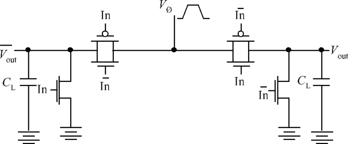
Fig. 1.
The adiabatic buffer/inverter circuit[9].
SEMICONDUCTOR INTEGRATED CIRCUITS
Jitendra Kanungo and S. Dasgupta
Corresponding author: S. Dasgupta, Email:jitendec@iitr.ernet.in, sudebfec@iitr.ernet.in
Abstract: This paper presents an analytical model to study the scaling trends in energy recovery logic. The energy performance of conventional CMOS and energy recovery logic are compared with scaling the design and technology parameters such as supply voltage, device threshold voltage and gate oxide thickness. The proposed analytical model is validated with simulation results at 90 nm and 65 nm CMOS technology nodes and predicts the scaling behavior accurately that help us to design an energy-efficient CMOS digital circuit design at the nanoscale. This research work shows the adiabatic switching as an ultra-low-power circuit technique for sub-100 nm digital CMOS circuit applications.
Keywords: adiabatic logic, energy efficient, energy recovery logic, low power digital CMOS logic
| [1] |
Kim S, Ziesler C H, Papaefthymiou M C. A true single-phase energy recovery multiplier. IEEE Trans Very Large Scale Integration (VLSI) Syst, 2003, 11(2):194 doi: 10.1109/TVLSI.2003.810795
|
| [2] |
Sathe V S, Chueh J Y, Papaefthyymiou M C. Energy-efficient GHz-class charge-recovery logic. IEEE J Solid-State Circuits, 2007, 42(1):38 doi: 10.1109/JSSC.2006.885053
|
| [3] |
Dickinson A G, Denkar J S. Adiabatic dynamic logic. IEEE J Solid-State Circuits, 1995, 30(3):311 doi: 10.1109/4.364447
|
| [4] |
Koller J G, Athas W C. Adiabatic switching, low energy computing, and the physics of storing and erasing information. Proc IEEE Workshop on Physics and Computation, Dallas, TX, 1992:267 http://ieeexplore.ieee.org/document/615554/?reload=true&arnumber=615554
|
| [5] |
Gong C S A, Shiue M T, Hong C T, et al. Analysis and design of efficient irreversible energy recovery logic in 0.18-μm CMOS. IEEE Trans Circuits Syst Ⅰ, 2008, 55(9):2995
|
| [6] |
Wisetphanichkij S, Dejhan K. The combinational and sequential adiabatic circuit design and its applications. Springer Journal of Circuits, Systems, and Signal Processing, 2009, 28(4):523 doi: 10.1007/s00034-009-9096-5
|
| [7] |
Chang L, Frank D J, Montoye R K, et al. Practical strategies for power-efficient computing technologies. Proc IEEE, 2010, 98(2):215 doi: 10.1109/JPROC.2009.2035451
|
| [8] |
Nayan A N, Takahashi Y, Sekine T. LSI implementation of a low-power 4×4-bit array two-phase clocked adiabatic static CMOS logic multiplier. Microelectron J, 2012, 43(4):244 doi: 10.1016/j.mejo.2011.12.013
|
| [9] |
Athas W C, Svensson L J, Koller J G, et al. Low-power digital systems based on adiabatic-switching principles. IEEE Trans Very Large Scale Integration (VLSI) Syst, 1994, 2(4):398 doi: 10.1109/92.335009
|
| [10] |
Rubinstein J, Penfield P, Horowitz M A. Signal delay in RC tree networks. IEEE Trans Comput Aided Design, 1983, 2(3):202 doi: 10.1109/TCAD.1983.1270037
|
| [11] |
Wyatt J L Jr. Signal delay in RC mesh networks. IEEE Trans Circuits Syst Ⅰ, 1985, 32(5):507 doi: 10.1109/TCS.1985.1085731
|
| [12] |
Hodges D A, Jackson H G, Saleh R A. Analysis and design of digital integrated circuits-in deep sub-micron technology. 3rd ed. Singapore:McGraw-Higher Education, 2003:326 http://bwrcs.eecs.berkeley.edu/Classes/icdesign/ee241_s04/lectures/Lecture1-Intro.pdf
|
| [13] |
Yeao K S, Roy K. Low-voltage, low-power VLSI subsystems. McGraw-Hill Professional Engineering, 2005:41 http://ci.nii.ac.jp/ncid/BA7051382X
|
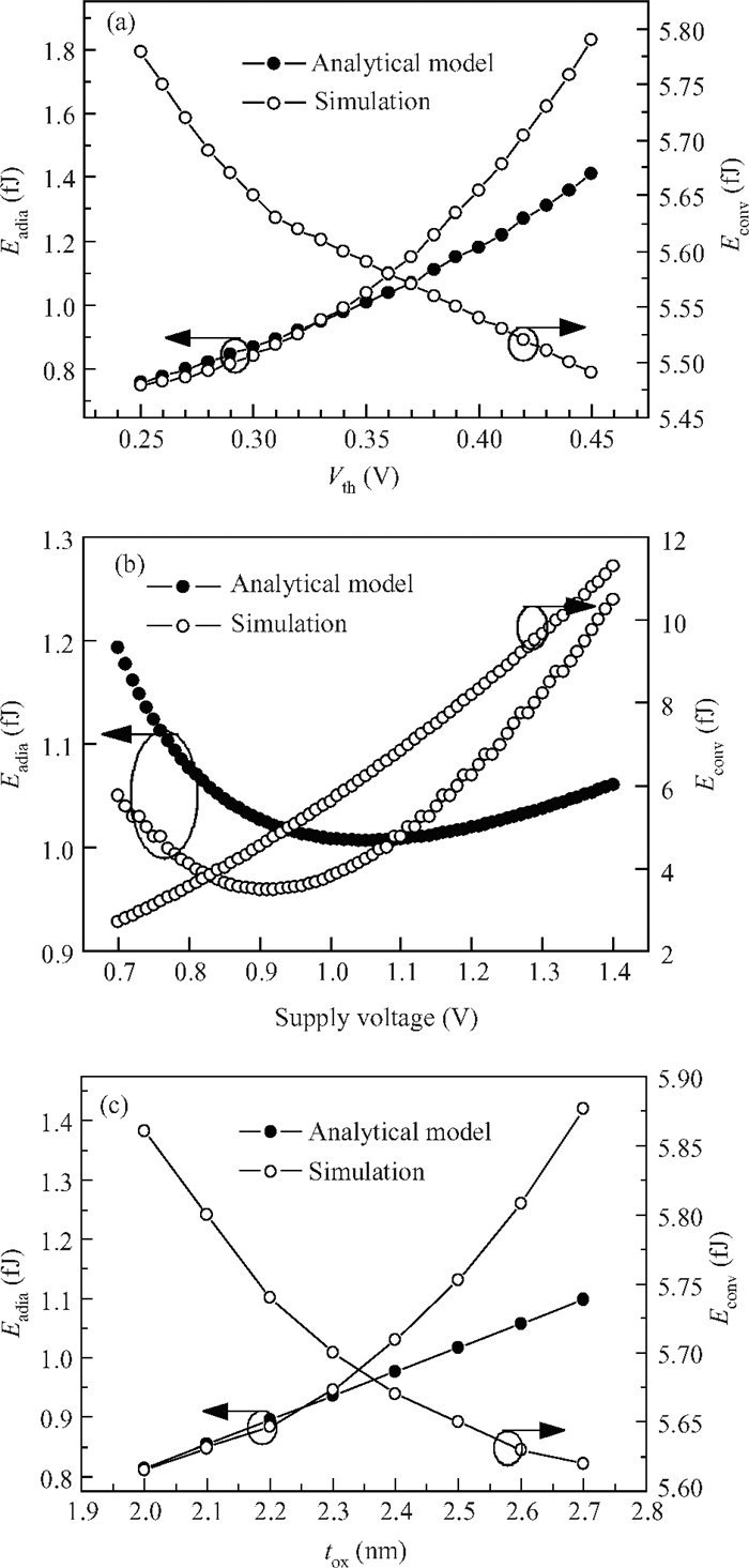
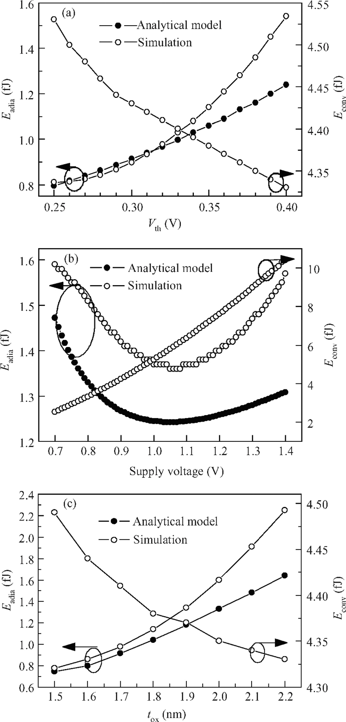
Table 1. The process parameters at 90 nm CMOS technology.

|
| [1] |
Kim S, Ziesler C H, Papaefthymiou M C. A true single-phase energy recovery multiplier. IEEE Trans Very Large Scale Integration (VLSI) Syst, 2003, 11(2):194 doi: 10.1109/TVLSI.2003.810795
|
| [2] |
Sathe V S, Chueh J Y, Papaefthyymiou M C. Energy-efficient GHz-class charge-recovery logic. IEEE J Solid-State Circuits, 2007, 42(1):38 doi: 10.1109/JSSC.2006.885053
|
| [3] |
Dickinson A G, Denkar J S. Adiabatic dynamic logic. IEEE J Solid-State Circuits, 1995, 30(3):311 doi: 10.1109/4.364447
|
| [4] |
Koller J G, Athas W C. Adiabatic switching, low energy computing, and the physics of storing and erasing information. Proc IEEE Workshop on Physics and Computation, Dallas, TX, 1992:267 http://ieeexplore.ieee.org/document/615554/?reload=true&arnumber=615554
|
| [5] |
Gong C S A, Shiue M T, Hong C T, et al. Analysis and design of efficient irreversible energy recovery logic in 0.18-μm CMOS. IEEE Trans Circuits Syst Ⅰ, 2008, 55(9):2995
|
| [6] |
Wisetphanichkij S, Dejhan K. The combinational and sequential adiabatic circuit design and its applications. Springer Journal of Circuits, Systems, and Signal Processing, 2009, 28(4):523 doi: 10.1007/s00034-009-9096-5
|
| [7] |
Chang L, Frank D J, Montoye R K, et al. Practical strategies for power-efficient computing technologies. Proc IEEE, 2010, 98(2):215 doi: 10.1109/JPROC.2009.2035451
|
| [8] |
Nayan A N, Takahashi Y, Sekine T. LSI implementation of a low-power 4×4-bit array two-phase clocked adiabatic static CMOS logic multiplier. Microelectron J, 2012, 43(4):244 doi: 10.1016/j.mejo.2011.12.013
|
| [9] |
Athas W C, Svensson L J, Koller J G, et al. Low-power digital systems based on adiabatic-switching principles. IEEE Trans Very Large Scale Integration (VLSI) Syst, 1994, 2(4):398 doi: 10.1109/92.335009
|
| [10] |
Rubinstein J, Penfield P, Horowitz M A. Signal delay in RC tree networks. IEEE Trans Comput Aided Design, 1983, 2(3):202 doi: 10.1109/TCAD.1983.1270037
|
| [11] |
Wyatt J L Jr. Signal delay in RC mesh networks. IEEE Trans Circuits Syst Ⅰ, 1985, 32(5):507 doi: 10.1109/TCS.1985.1085731
|
| [12] |
Hodges D A, Jackson H G, Saleh R A. Analysis and design of digital integrated circuits-in deep sub-micron technology. 3rd ed. Singapore:McGraw-Higher Education, 2003:326 http://bwrcs.eecs.berkeley.edu/Classes/icdesign/ee241_s04/lectures/Lecture1-Intro.pdf
|
| [13] |
Yeao K S, Roy K. Low-voltage, low-power VLSI subsystems. McGraw-Hill Professional Engineering, 2005:41 http://ci.nii.ac.jp/ncid/BA7051382X
|


Article views: 2770 Times PDF downloads: 12 Times Cited by: 0 Times
Received: 16 January 2013 Revised: Online: Published: 01 August 2013
| Citation: |
Jitendra Kanungo, S. Dasgupta. Scaling trends in energy recovery logic:an analytical approach[J]. Journal of Semiconductors, 2013, 34(8): 085001. doi: 10.1088/1674-4926/34/8/085001
****
J Kanungo, S. Dasgupta. Scaling trends in energy recovery logic:an analytical approach[J]. J. Semicond., 2013, 34(8): 085001. doi: 10.1088/1674-4926/34/8/085001.

|
| [1] |
Kim S, Ziesler C H, Papaefthymiou M C. A true single-phase energy recovery multiplier. IEEE Trans Very Large Scale Integration (VLSI) Syst, 2003, 11(2):194 doi: 10.1109/TVLSI.2003.810795
|
| [2] |
Sathe V S, Chueh J Y, Papaefthyymiou M C. Energy-efficient GHz-class charge-recovery logic. IEEE J Solid-State Circuits, 2007, 42(1):38 doi: 10.1109/JSSC.2006.885053
|
| [3] |
Dickinson A G, Denkar J S. Adiabatic dynamic logic. IEEE J Solid-State Circuits, 1995, 30(3):311 doi: 10.1109/4.364447
|
| [4] |
Koller J G, Athas W C. Adiabatic switching, low energy computing, and the physics of storing and erasing information. Proc IEEE Workshop on Physics and Computation, Dallas, TX, 1992:267 http://ieeexplore.ieee.org/document/615554/?reload=true&arnumber=615554
|
| [5] |
Gong C S A, Shiue M T, Hong C T, et al. Analysis and design of efficient irreversible energy recovery logic in 0.18-μm CMOS. IEEE Trans Circuits Syst Ⅰ, 2008, 55(9):2995
|
| [6] |
Wisetphanichkij S, Dejhan K. The combinational and sequential adiabatic circuit design and its applications. Springer Journal of Circuits, Systems, and Signal Processing, 2009, 28(4):523 doi: 10.1007/s00034-009-9096-5
|
| [7] |
Chang L, Frank D J, Montoye R K, et al. Practical strategies for power-efficient computing technologies. Proc IEEE, 2010, 98(2):215 doi: 10.1109/JPROC.2009.2035451
|
| [8] |
Nayan A N, Takahashi Y, Sekine T. LSI implementation of a low-power 4×4-bit array two-phase clocked adiabatic static CMOS logic multiplier. Microelectron J, 2012, 43(4):244 doi: 10.1016/j.mejo.2011.12.013
|
| [9] |
Athas W C, Svensson L J, Koller J G, et al. Low-power digital systems based on adiabatic-switching principles. IEEE Trans Very Large Scale Integration (VLSI) Syst, 1994, 2(4):398 doi: 10.1109/92.335009
|
| [10] |
Rubinstein J, Penfield P, Horowitz M A. Signal delay in RC tree networks. IEEE Trans Comput Aided Design, 1983, 2(3):202 doi: 10.1109/TCAD.1983.1270037
|
| [11] |
Wyatt J L Jr. Signal delay in RC mesh networks. IEEE Trans Circuits Syst Ⅰ, 1985, 32(5):507 doi: 10.1109/TCS.1985.1085731
|
| [12] |
Hodges D A, Jackson H G, Saleh R A. Analysis and design of digital integrated circuits-in deep sub-micron technology. 3rd ed. Singapore:McGraw-Higher Education, 2003:326 http://bwrcs.eecs.berkeley.edu/Classes/icdesign/ee241_s04/lectures/Lecture1-Intro.pdf
|
| [13] |
Yeao K S, Roy K. Low-voltage, low-power VLSI subsystems. McGraw-Hill Professional Engineering, 2005:41 http://ci.nii.ac.jp/ncid/BA7051382X
|

 WeChat ID
Journal of Semiconductors © 2017 All Rights Reserved 京ICP备05085259号-2

 DownLoad:

