Fig. 1.
Block diagram of the front end system.
SEMICONDUCTOR INTEGRATED CIRCUITS
Jia Cao, Zhiqun Li, Qin Li, Liang Chen, Meng Zhang, Chenjian Wu, Chong Wang and Zhigong Wang
Corresponding author: Cao Jia, Email:caojia.seu@gmail.com
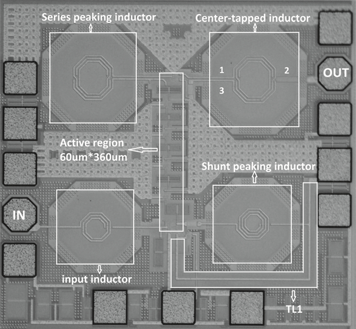
Abstract: This paper presents a high-gain wideband low-noise IF amplifier aimed for the ALMA front end system using 90-nm LP CMOS technology. A topology of three optimized cascading stages is proposed to achieve a flat and wideband gain. Incorporating an input inductor and a gate-inductive gain-peaking inductor, the active shunt feedback technique is employed to extend the matching bandwidth and optimize the noise figure. The circuit achieves a flat gain of 30.5 dB with 3 dB bandwidth of 1-16 GHz and a minimum noise figure of 3.76 dB. Under 1.2 V supply voltage, the proposed IF amplifier consumes 42 mW DC power. The chip die including pads takes up 0.53 mm2, while the active area is only 0.022 mm2.
Key words: CMOS, IF amplifier, high gain, low noise amplifier, wideband, peaking technique, cascading amplifier
| [1] | |
| [2] |
Lopez-Fernandez I, Daniel J, Puyol G. Development of cryogenic IF low-noise 4-12 GHz amplifiers for ALMA radio astronomy receivers. IEEE MTT-S Int Microw Symp Dig, 2006:1907 http://ieeexplore.ieee.org/document/4015330/keywords
|
| [3] |
Borremans J, Wambacq P, Soens C. Low-area active-feedback low-noise amplifier design in scaled digital CMOS. IEEE J Solid-State Circuits, 2008, 43(11):2022 http://ieeexplore.ieee.org/document/4685422/keywords
|
| [4] |
Okushima M, Borremans J, Linten D, et al. A DC-to-22 GHz 8.4 mW compact dual-feedback wideband LNA in 90 nm digital CMOS. IEEE Radio Freq Integr Circuits Symp, 2009:295 http://ieeexplore.ieee.org/document/5135543/
|
| [5] |
Chen W H, Liu G. A highly linear broadband CMOS LNA employing noise and distortion cancellation. IEEE J Solid-State Circuits, 2008, 43(5):1164 doi: 10.1109/JSSC.2008.920335
|
| [6] |
Blaakmeer S C, Klumperink E A M. Wideband Balun-LNA with simultaneous output balancing, noise-canceling and distortion-canceling. IEEE J Solid-State Circuits, 2008, 43(6):1341 doi: 10.1109/JSSC.2008.922736
|
| [7] |
Shaeffer D K, Lee T H. A 1.5-V 1.5-GHz CMOS low noise amplifier. IEEE J Solid-State Circuits, 1997, 32(5):745 doi: 10.1109/4.568846
|
| [8] |
Lee T H. The design of CMOS radio-frequency integrated circuits. 2nd ed. Communications Engineer, 2004
|
| [9] |
Chen H K, Lin Y S. Analysis and design of a 1.6-28-GHz compact wideband LNA in 90-nm CMOS using a π -match input network. IEEE Trans Microw Theory Tech, 2010, 58(8):2092 doi: 10.1109/TMTT.2010.2052406
|
| [10] |
Chen M, Lin J. A 0.1-20 GHz low-power self-biased resistive-feedback LNA in 90 nm digital CMOS. IEEE Microw Wireless Compon Lett, 2009, 19(5):323 doi: 10.1109/LMWC.2009.2017608
|
| [11] |
Chang P Y, Hsu S S H. A compact 0.1-14-GHz ultra-wideband low-noise amplifier in 0.13-μm CMOS. IEEE Trans Microw Theory Tech, 2010, 58(10):2575
|
| [12] |
Sapone G, Palmisano G. A 3-10-GHz low-power CMOS low-noise amplifier for ultra-wideband communication. IEEE Trans Microw Theory Tech, 2011, 59(3):678 doi: 10.1109/TMTT.2010.2090357
|
| [13] |
Hsieh H H, Lu L H. A 40-GHz low-noise amplifier with a positive-feedback network in 0.18-μm CMOS. IEEE Trans Microw Theory Tech, 2009, 57(8):1895 doi: 10.1109/TMTT.2009.2025418
|
| [14] |
Lin Y S, Chen C Z, Yang H Y, et al. Analysis anddesign of a CMOS UWB LNA with dual-RLC-branch wideband input matching network. IEEE Trans Microw Theory Tech, 2010, 58(2):287 doi: 10.1109/TMTT.2009.2037863
|
| [15] |
El-Gabaly A M, Saavedra C E. Broadband low-noise amplifier with fast power switching for 3.1-10.6-GHz ultra-wideband applications. IEEE Trans Microw Theory Tech, 2011, 59(12):3146 doi: 10.1109/TMTT.2011.2169277
|
| [16] |
Heydari P. Design and analysis of a performance-optimized CMOS UWB distributed LNA. IEEE J Solid-State Circuits, 2007, 42(9):1892 doi: 10.1109/JSSC.2007.903046
|
| [17] |
He K C, Li M T, Li C M, et al. Parallel-RC feedback low-noise amplifier for UWB applications. IEEE Trans Circuits Syst Ⅱ, Exp Briefs, 2010, 57(8):582 doi: 10.1109/TCSII.2010.2050943
|
| [18] |
Lai Q T, Mao J F. A 0.5-11 GHz CMOS low noise amplifier using dual-channel shunt technique. IEEE Microw Wireless Compon Lett, 2010, 19(5):280 http://ieeexplore.ieee.org/document/5443550/?tp=&arnumber=5443550&queryText%3D(dual-channel%20cmos%20)
|
| [19] |
Pepe D, Zito D. 22.7-dB gain-19.7-dBm ICP1dB UWB CMOS LNA. IEEE Trans Circuits Syst Ⅱ, Exp Briefs, 2009, 56(9):689
|
| [20] |
Fang C, Law C L, Hwang J. A 3.1-10.6 GHz ultra-wideband low noise amplifier with 13-dB gain, 3.4-dB noise figure, and consumes only 12.9 mW of DC power. IEEE Microw Wireless Compon Lett, 2007, 17(4):295 doi: 10.1109/LMWC.2007.892984
|
| [21] |
Chen K H, Lu J H, Chen B J, et al. An ultra-wide-band 0.4-10-GHz LNA in 0.18-μm CMOS. IEEE Trans Circuits Syst Ⅱ, Exp Briefs, 2007, 54(3):217 doi: 10.1109/TCSII.2006.886880
|

Table 1. Performance Summary and Comparison with Prior Wideband Amplifiers.

|
| [1] | |
| [2] |
Lopez-Fernandez I, Daniel J, Puyol G. Development of cryogenic IF low-noise 4-12 GHz amplifiers for ALMA radio astronomy receivers. IEEE MTT-S Int Microw Symp Dig, 2006:1907 http://ieeexplore.ieee.org/document/4015330/keywords
|
| [3] |
Borremans J, Wambacq P, Soens C. Low-area active-feedback low-noise amplifier design in scaled digital CMOS. IEEE J Solid-State Circuits, 2008, 43(11):2022 http://ieeexplore.ieee.org/document/4685422/keywords
|
| [4] |
Okushima M, Borremans J, Linten D, et al. A DC-to-22 GHz 8.4 mW compact dual-feedback wideband LNA in 90 nm digital CMOS. IEEE Radio Freq Integr Circuits Symp, 2009:295 http://ieeexplore.ieee.org/document/5135543/
|
| [5] |
Chen W H, Liu G. A highly linear broadband CMOS LNA employing noise and distortion cancellation. IEEE J Solid-State Circuits, 2008, 43(5):1164 doi: 10.1109/JSSC.2008.920335
|
| [6] |
Blaakmeer S C, Klumperink E A M. Wideband Balun-LNA with simultaneous output balancing, noise-canceling and distortion-canceling. IEEE J Solid-State Circuits, 2008, 43(6):1341 doi: 10.1109/JSSC.2008.922736
|
| [7] |
Shaeffer D K, Lee T H. A 1.5-V 1.5-GHz CMOS low noise amplifier. IEEE J Solid-State Circuits, 1997, 32(5):745 doi: 10.1109/4.568846
|
| [8] |
Lee T H. The design of CMOS radio-frequency integrated circuits. 2nd ed. Communications Engineer, 2004
|
| [9] |
Chen H K, Lin Y S. Analysis and design of a 1.6-28-GHz compact wideband LNA in 90-nm CMOS using a π -match input network. IEEE Trans Microw Theory Tech, 2010, 58(8):2092 doi: 10.1109/TMTT.2010.2052406
|
| [10] |
Chen M, Lin J. A 0.1-20 GHz low-power self-biased resistive-feedback LNA in 90 nm digital CMOS. IEEE Microw Wireless Compon Lett, 2009, 19(5):323 doi: 10.1109/LMWC.2009.2017608
|
| [11] |
Chang P Y, Hsu S S H. A compact 0.1-14-GHz ultra-wideband low-noise amplifier in 0.13-μm CMOS. IEEE Trans Microw Theory Tech, 2010, 58(10):2575
|
| [12] |
Sapone G, Palmisano G. A 3-10-GHz low-power CMOS low-noise amplifier for ultra-wideband communication. IEEE Trans Microw Theory Tech, 2011, 59(3):678 doi: 10.1109/TMTT.2010.2090357
|
| [13] |
Hsieh H H, Lu L H. A 40-GHz low-noise amplifier with a positive-feedback network in 0.18-μm CMOS. IEEE Trans Microw Theory Tech, 2009, 57(8):1895 doi: 10.1109/TMTT.2009.2025418
|
| [14] |
Lin Y S, Chen C Z, Yang H Y, et al. Analysis anddesign of a CMOS UWB LNA with dual-RLC-branch wideband input matching network. IEEE Trans Microw Theory Tech, 2010, 58(2):287 doi: 10.1109/TMTT.2009.2037863
|
| [15] |
El-Gabaly A M, Saavedra C E. Broadband low-noise amplifier with fast power switching for 3.1-10.6-GHz ultra-wideband applications. IEEE Trans Microw Theory Tech, 2011, 59(12):3146 doi: 10.1109/TMTT.2011.2169277
|
| [16] |
Heydari P. Design and analysis of a performance-optimized CMOS UWB distributed LNA. IEEE J Solid-State Circuits, 2007, 42(9):1892 doi: 10.1109/JSSC.2007.903046
|
| [17] |
He K C, Li M T, Li C M, et al. Parallel-RC feedback low-noise amplifier for UWB applications. IEEE Trans Circuits Syst Ⅱ, Exp Briefs, 2010, 57(8):582 doi: 10.1109/TCSII.2010.2050943
|
| [18] |
Lai Q T, Mao J F. A 0.5-11 GHz CMOS low noise amplifier using dual-channel shunt technique. IEEE Microw Wireless Compon Lett, 2010, 19(5):280 http://ieeexplore.ieee.org/document/5443550/?tp=&arnumber=5443550&queryText%3D(dual-channel%20cmos%20)
|
| [19] |
Pepe D, Zito D. 22.7-dB gain-19.7-dBm ICP1dB UWB CMOS LNA. IEEE Trans Circuits Syst Ⅱ, Exp Briefs, 2009, 56(9):689
|
| [20] |
Fang C, Law C L, Hwang J. A 3.1-10.6 GHz ultra-wideband low noise amplifier with 13-dB gain, 3.4-dB noise figure, and consumes only 12.9 mW of DC power. IEEE Microw Wireless Compon Lett, 2007, 17(4):295 doi: 10.1109/LMWC.2007.892984
|
| [21] |
Chen K H, Lu J H, Chen B J, et al. An ultra-wide-band 0.4-10-GHz LNA in 0.18-μm CMOS. IEEE Trans Circuits Syst Ⅱ, Exp Briefs, 2007, 54(3):217 doi: 10.1109/TCSII.2006.886880
|


Article views: 3241 Times PDF downloads: 29 Times Cited by: 0 Times
Received: 12 December 2012 Revised: 04 January 2013 Online: Published: 01 August 2013
| Citation: |
Jia Cao, Zhiqun Li, Qin Li, Liang Chen, Meng Zhang, Chenjian Wu, Chong Wang, Zhigong Wang. A 30-dB 1-16-GHz low noise IF amplifier in 90-nm CMOS[J]. Journal of Semiconductors, 2013, 34(8): 085010. doi: 10.1088/1674-4926/34/8/085010
****
J Cao, Z Q Li, Q Li, L Chen, M Zhang, C J Wu, C Wang, Z G Wang. A 30-dB 1-16-GHz low noise IF amplifier in 90-nm CMOS[J]. J. Semicond., 2013, 34(8): 085010. doi: 10.1088/1674-4926/34/8/085010.

|
| [1] | |
| [2] |
Lopez-Fernandez I, Daniel J, Puyol G. Development of cryogenic IF low-noise 4-12 GHz amplifiers for ALMA radio astronomy receivers. IEEE MTT-S Int Microw Symp Dig, 2006:1907 http://ieeexplore.ieee.org/document/4015330/keywords
|
| [3] |
Borremans J, Wambacq P, Soens C. Low-area active-feedback low-noise amplifier design in scaled digital CMOS. IEEE J Solid-State Circuits, 2008, 43(11):2022 http://ieeexplore.ieee.org/document/4685422/keywords
|
| [4] |
Okushima M, Borremans J, Linten D, et al. A DC-to-22 GHz 8.4 mW compact dual-feedback wideband LNA in 90 nm digital CMOS. IEEE Radio Freq Integr Circuits Symp, 2009:295 http://ieeexplore.ieee.org/document/5135543/
|
| [5] |
Chen W H, Liu G. A highly linear broadband CMOS LNA employing noise and distortion cancellation. IEEE J Solid-State Circuits, 2008, 43(5):1164 doi: 10.1109/JSSC.2008.920335
|
| [6] |
Blaakmeer S C, Klumperink E A M. Wideband Balun-LNA with simultaneous output balancing, noise-canceling and distortion-canceling. IEEE J Solid-State Circuits, 2008, 43(6):1341 doi: 10.1109/JSSC.2008.922736
|
| [7] |
Shaeffer D K, Lee T H. A 1.5-V 1.5-GHz CMOS low noise amplifier. IEEE J Solid-State Circuits, 1997, 32(5):745 doi: 10.1109/4.568846
|
| [8] |
Lee T H. The design of CMOS radio-frequency integrated circuits. 2nd ed. Communications Engineer, 2004
|
| [9] |
Chen H K, Lin Y S. Analysis and design of a 1.6-28-GHz compact wideband LNA in 90-nm CMOS using a π -match input network. IEEE Trans Microw Theory Tech, 2010, 58(8):2092 doi: 10.1109/TMTT.2010.2052406
|
| [10] |
Chen M, Lin J. A 0.1-20 GHz low-power self-biased resistive-feedback LNA in 90 nm digital CMOS. IEEE Microw Wireless Compon Lett, 2009, 19(5):323 doi: 10.1109/LMWC.2009.2017608
|
| [11] |
Chang P Y, Hsu S S H. A compact 0.1-14-GHz ultra-wideband low-noise amplifier in 0.13-μm CMOS. IEEE Trans Microw Theory Tech, 2010, 58(10):2575
|
| [12] |
Sapone G, Palmisano G. A 3-10-GHz low-power CMOS low-noise amplifier for ultra-wideband communication. IEEE Trans Microw Theory Tech, 2011, 59(3):678 doi: 10.1109/TMTT.2010.2090357
|
| [13] |
Hsieh H H, Lu L H. A 40-GHz low-noise amplifier with a positive-feedback network in 0.18-μm CMOS. IEEE Trans Microw Theory Tech, 2009, 57(8):1895 doi: 10.1109/TMTT.2009.2025418
|
| [14] |
Lin Y S, Chen C Z, Yang H Y, et al. Analysis anddesign of a CMOS UWB LNA with dual-RLC-branch wideband input matching network. IEEE Trans Microw Theory Tech, 2010, 58(2):287 doi: 10.1109/TMTT.2009.2037863
|
| [15] |
El-Gabaly A M, Saavedra C E. Broadband low-noise amplifier with fast power switching for 3.1-10.6-GHz ultra-wideband applications. IEEE Trans Microw Theory Tech, 2011, 59(12):3146 doi: 10.1109/TMTT.2011.2169277
|
| [16] |
Heydari P. Design and analysis of a performance-optimized CMOS UWB distributed LNA. IEEE J Solid-State Circuits, 2007, 42(9):1892 doi: 10.1109/JSSC.2007.903046
|
| [17] |
He K C, Li M T, Li C M, et al. Parallel-RC feedback low-noise amplifier for UWB applications. IEEE Trans Circuits Syst Ⅱ, Exp Briefs, 2010, 57(8):582 doi: 10.1109/TCSII.2010.2050943
|
| [18] |
Lai Q T, Mao J F. A 0.5-11 GHz CMOS low noise amplifier using dual-channel shunt technique. IEEE Microw Wireless Compon Lett, 2010, 19(5):280 http://ieeexplore.ieee.org/document/5443550/?tp=&arnumber=5443550&queryText%3D(dual-channel%20cmos%20)
|
| [19] |
Pepe D, Zito D. 22.7-dB gain-19.7-dBm ICP1dB UWB CMOS LNA. IEEE Trans Circuits Syst Ⅱ, Exp Briefs, 2009, 56(9):689
|
| [20] |
Fang C, Law C L, Hwang J. A 3.1-10.6 GHz ultra-wideband low noise amplifier with 13-dB gain, 3.4-dB noise figure, and consumes only 12.9 mW of DC power. IEEE Microw Wireless Compon Lett, 2007, 17(4):295 doi: 10.1109/LMWC.2007.892984
|
| [21] |
Chen K H, Lu J H, Chen B J, et al. An ultra-wide-band 0.4-10-GHz LNA in 0.18-μm CMOS. IEEE Trans Circuits Syst Ⅱ, Exp Briefs, 2007, 54(3):217 doi: 10.1109/TCSII.2006.886880
|

 WeChat ID
Journal of Semiconductors © 2017 All Rights Reserved 京ICP备05085259号-2

 DownLoad: