


Fig. 1.
Procedure for fabricating Ti-diffused LN ridge waveguides.
SEMICONDUCTOR TECHNOLOGY
Jianjie Wu, Jinyang Li, Yanqing Yao and Zhimei Qi
Corresponding author: Qi Zhimei, Email:zhimei-qi@mail.ie.ac.cn
Abstract: Reactive ion etching (RIE) of LiNbO3 (LN) in SF6 plasma atmosphere was studied for optimizing the preparation conditions for LN ridge waveguides. The samples to be etched are Ti-diffused LN slab waveguides overlaid with a chromium film mask that has a Mach-Zehnder interferometer (MZI) array pattern. The experimental results indicate that the LN-etching rate (RLN) and the Cr-etching rate (RCr) as well as the rate ratio RLN/RCr increase with either increasing the radio-frequency (RF) power at a given SF6 flow rate or increasing the SF6 flow rate at a fixed RF power. The maximum values of RLN=43.2 nm/min and RLN/RCr=3.27 were achieved with 300 W RF power and 40 sccm SF6 flow. When the SF6 flow rate exceeds 40 sccm, an increase in the flow rate causes the etching rates and the rate ratio to decrease. The scanning electron microscope images of the LN ridge prepared after ~ 20 min etching show that the ridge height is 680 nm and the sidewall slope angle is about 60°.
Keywords: reactive ion etching, Ti-diffused LiNbO3 slab waveguide, optimal etching parameters, ridge waveguide
| [1] |
Kazuto N, Osamu M, Hiroshi M, et al. A broadband Ti:LiNbO3 optical modulator with a ridge structure. J Lightwave Technol, 1995, 13(6):1164 doi: 10.1109/50.390234
|
| [2] |
Yi K W, Way S W. Design and fabrication of sidewalls-extended electrode configuration for ridged lithium niobate electrooptical modulator. J Lightwave Technol, 2008, 26(2):286 doi: 10.1109/JLT.2007.909863
|
| [3] |
Miguel G, Hui H, Rodrìguezgarcìa J, et al. Design and fabrication of novel ridge guide modulators in lithium niobate. J Lightwave Technol, 2009, 27(24):5690 doi: 10.1109/JLT.2009.2034756
|
| [4] |
Cheng F S, Li Q C. Integrated electrooptic M-Z modulator with ridge structure in X-cut LiNbO3. Chinese Journal of Lasers, 2002, 29(3):209
|
| [5] |
Zhang Y J, Chen C H, Zhong J J, et al. Design and experiment of acousto-optic waveguide phase modulator in electro-optic integrated acceleration seismic geophone. Nanotechnology and Precision Engineering, 2005, 3(1):64
|
| [6] |
Shih J C, Ching L T, Yih B L, et al. Improved electrooptic modulator with ridge structure in X-Cut LiNbO3. J Lightwave Technol, 1999, 17(5):843 doi: 10.1109/50.762902
|
| [7] |
Rei S C, Tzyy J W, Way S W. Wet-etched ridge waveguides in Y-cut lithium niobate. J Lightwave Technol, 1997, 15(10):1880 doi: 10.1109/50.633578
|
| [8] |
Zhao Y, Jiang X, Li C Y, et al. RIE of SiO2 nanoparticles and its application in preparation of silicon nanopillar array. Nanotechnology and Precision Engineering, 2009, 7(6):515
|
| [9] |
Yao Y Q, Li J Y, Wu J J, et al. Research development on LiNbO3 dry etching. Micronanoelectron Technol, 2012, 49(3):197
|
| [10] |
Hong T, Zhang Y G, Liu T D. Reactive ion etching of GaAs, GaSb, InP and InAs in Cl2/Ar plasma. Semicond Photonics Technol, 2004, 10(3):203
|
| [11] |
Ding H T, Yang Z C, Zhang M L, et al. Experimental study on the footing effect for SOG structures using DRIE. Journal of Semiconductors, 2008, 29(6):1088 http://www.jos.ac.cn/bdtxbcn/ch/reader/view_abstract.aspx?file_no=07121904&flag=1
|
| [12] |
Sarach B, Laurent R, Jean Y R, et al. Highly selective electroplated nickel mask for lithium niobate dry etching. J Appl Phys, 2009, 105(9):094109 doi: 10.1063/1.3125315
|
| [13] |
Jiang W J, Xu C, Deng C, et al. GaP surface profile control through ICP etching. Nanotechnology and Precision Engineering, 2010, 8(3):281
|
| [14] |
Meng L L, Chen Y X, Ma L, et al. ICP dry etching ITO to improve the performance of GaN-based LEDs. Journal of Semiconductors, 2011, 32(1):014010 doi: 10.1088/1674-4926/32/1/014010
|
| [15] |
Zhao J H, Liu X H, Qing H, et al. Lithium niobate ridge waveguides fabricated by ion implantation followed by ion beam etching. J Lightwave Technol, 2010, 28(13):1913 doi: 10.1109/JLT.2010.2050296
|
| [16] |
Meriche F, Boudrioua A, Kremer R, et al. Fabrication and investigation of 1D and 2D structures in LiNbO3 thin films by pulsed laser ablation. Opt Mater, 2010, 32(11):1427 doi: 10.1016/j.optmat.2010.05.010
|
| [17] |
Vijay S, Arnan M, Lam B, et al. Etching of lithium niobate using standard Ti indiffusion technique. Appl Phys Lett, 2007, 91(23):231921 doi: 10.1063/1.2821111
|
| [18] |
Xie J, Jiang S H, Wang J J, et al. Investigation on etch performance of focused ion beam. Chinese Journal of Semiconductors, 2001, 11(2):151
|
| [19] |
Chen F, Liu R P, Qi Z M. Design, fabrication and characterization of LiNbO3-based integrated optical waveguide Mach-Zehnder interferometer. Acta Optica Sinica, 2011, 31(5):0513001 doi: 10.3788/AOS
|
| [20] |
Li J Y, Yao Y Q, Wu J J, et al. Theoretical analysis and preliminary fabrication of Ti-diffused LiNbO3 ridge waveguides. Acta Optica Sinica, 2013, 33(2):0223001 doi: 10.3788/AOS
|
| [21] |
Hu H, Milenin A P, Wehrspohn R B, et al. Plasma etching of proton-exchanged lithium niobate. J Vac Sci Technol A, 2006, 24(4):1012 doi: 10.1116/1.2207150
|


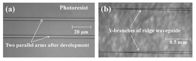
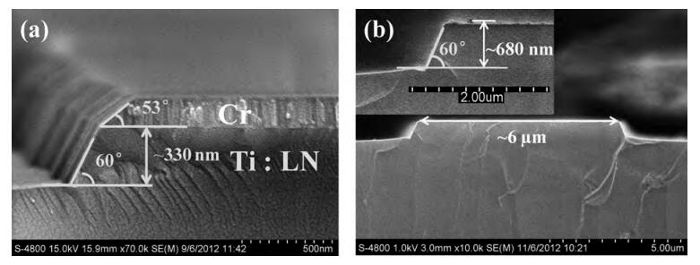
Table 1.
LN-etching rate (

|
Table 2.

|
| [1] |
Kazuto N, Osamu M, Hiroshi M, et al. A broadband Ti:LiNbO3 optical modulator with a ridge structure. J Lightwave Technol, 1995, 13(6):1164 doi: 10.1109/50.390234
|
| [2] |
Yi K W, Way S W. Design and fabrication of sidewalls-extended electrode configuration for ridged lithium niobate electrooptical modulator. J Lightwave Technol, 2008, 26(2):286 doi: 10.1109/JLT.2007.909863
|
| [3] |
Miguel G, Hui H, Rodrìguezgarcìa J, et al. Design and fabrication of novel ridge guide modulators in lithium niobate. J Lightwave Technol, 2009, 27(24):5690 doi: 10.1109/JLT.2009.2034756
|
| [4] |
Cheng F S, Li Q C. Integrated electrooptic M-Z modulator with ridge structure in X-cut LiNbO3. Chinese Journal of Lasers, 2002, 29(3):209
|
| [5] |
Zhang Y J, Chen C H, Zhong J J, et al. Design and experiment of acousto-optic waveguide phase modulator in electro-optic integrated acceleration seismic geophone. Nanotechnology and Precision Engineering, 2005, 3(1):64
|
| [6] |
Shih J C, Ching L T, Yih B L, et al. Improved electrooptic modulator with ridge structure in X-Cut LiNbO3. J Lightwave Technol, 1999, 17(5):843 doi: 10.1109/50.762902
|
| [7] |
Rei S C, Tzyy J W, Way S W. Wet-etched ridge waveguides in Y-cut lithium niobate. J Lightwave Technol, 1997, 15(10):1880 doi: 10.1109/50.633578
|
| [8] |
Zhao Y, Jiang X, Li C Y, et al. RIE of SiO2 nanoparticles and its application in preparation of silicon nanopillar array. Nanotechnology and Precision Engineering, 2009, 7(6):515
|
| [9] |
Yao Y Q, Li J Y, Wu J J, et al. Research development on LiNbO3 dry etching. Micronanoelectron Technol, 2012, 49(3):197
|
| [10] |
Hong T, Zhang Y G, Liu T D. Reactive ion etching of GaAs, GaSb, InP and InAs in Cl2/Ar plasma. Semicond Photonics Technol, 2004, 10(3):203
|
| [11] |
Ding H T, Yang Z C, Zhang M L, et al. Experimental study on the footing effect for SOG structures using DRIE. Journal of Semiconductors, 2008, 29(6):1088 http://www.jos.ac.cn/bdtxbcn/ch/reader/view_abstract.aspx?file_no=07121904&flag=1
|
| [12] |
Sarach B, Laurent R, Jean Y R, et al. Highly selective electroplated nickel mask for lithium niobate dry etching. J Appl Phys, 2009, 105(9):094109 doi: 10.1063/1.3125315
|
| [13] |
Jiang W J, Xu C, Deng C, et al. GaP surface profile control through ICP etching. Nanotechnology and Precision Engineering, 2010, 8(3):281
|
| [14] |
Meng L L, Chen Y X, Ma L, et al. ICP dry etching ITO to improve the performance of GaN-based LEDs. Journal of Semiconductors, 2011, 32(1):014010 doi: 10.1088/1674-4926/32/1/014010
|
| [15] |
Zhao J H, Liu X H, Qing H, et al. Lithium niobate ridge waveguides fabricated by ion implantation followed by ion beam etching. J Lightwave Technol, 2010, 28(13):1913 doi: 10.1109/JLT.2010.2050296
|
| [16] |
Meriche F, Boudrioua A, Kremer R, et al. Fabrication and investigation of 1D and 2D structures in LiNbO3 thin films by pulsed laser ablation. Opt Mater, 2010, 32(11):1427 doi: 10.1016/j.optmat.2010.05.010
|
| [17] |
Vijay S, Arnan M, Lam B, et al. Etching of lithium niobate using standard Ti indiffusion technique. Appl Phys Lett, 2007, 91(23):231921 doi: 10.1063/1.2821111
|
| [18] |
Xie J, Jiang S H, Wang J J, et al. Investigation on etch performance of focused ion beam. Chinese Journal of Semiconductors, 2001, 11(2):151
|
| [19] |
Chen F, Liu R P, Qi Z M. Design, fabrication and characterization of LiNbO3-based integrated optical waveguide Mach-Zehnder interferometer. Acta Optica Sinica, 2011, 31(5):0513001 doi: 10.3788/AOS
|
| [20] |
Li J Y, Yao Y Q, Wu J J, et al. Theoretical analysis and preliminary fabrication of Ti-diffused LiNbO3 ridge waveguides. Acta Optica Sinica, 2013, 33(2):0223001 doi: 10.3788/AOS
|
| [21] |
Hu H, Milenin A P, Wehrspohn R B, et al. Plasma etching of proton-exchanged lithium niobate. J Vac Sci Technol A, 2006, 24(4):1012 doi: 10.1116/1.2207150
|


Article views: 3591 Times PDF downloads: 45 Times Cited by: 0 Times
Received: 27 December 2012 Revised: 30 January 2013 Online: Published: 01 August 2013
| Citation: |
Jianjie Wu, Jinyang Li, Yanqing Yao, Zhimei Qi. Reactive ion etching of Ti-diffused LiNbO3 slab waveguides[J]. Journal of Semiconductors, 2013, 34(8): 086001. doi: 10.1088/1674-4926/34/8/086001
****
J J Wu, J Y Li, Y Q Yao, Z M Qi. Reactive ion etching of Ti-diffused LiNbO3 slab waveguides[J]. J. Semicond., 2013, 34(8): 086001. doi: 10.1088/1674-4926/34/8/086001.

|
| [1] |
Kazuto N, Osamu M, Hiroshi M, et al. A broadband Ti:LiNbO3 optical modulator with a ridge structure. J Lightwave Technol, 1995, 13(6):1164 doi: 10.1109/50.390234
|
| [2] |
Yi K W, Way S W. Design and fabrication of sidewalls-extended electrode configuration for ridged lithium niobate electrooptical modulator. J Lightwave Technol, 2008, 26(2):286 doi: 10.1109/JLT.2007.909863
|
| [3] |
Miguel G, Hui H, Rodrìguezgarcìa J, et al. Design and fabrication of novel ridge guide modulators in lithium niobate. J Lightwave Technol, 2009, 27(24):5690 doi: 10.1109/JLT.2009.2034756
|
| [4] |
Cheng F S, Li Q C. Integrated electrooptic M-Z modulator with ridge structure in X-cut LiNbO3. Chinese Journal of Lasers, 2002, 29(3):209
|
| [5] |
Zhang Y J, Chen C H, Zhong J J, et al. Design and experiment of acousto-optic waveguide phase modulator in electro-optic integrated acceleration seismic geophone. Nanotechnology and Precision Engineering, 2005, 3(1):64
|
| [6] |
Shih J C, Ching L T, Yih B L, et al. Improved electrooptic modulator with ridge structure in X-Cut LiNbO3. J Lightwave Technol, 1999, 17(5):843 doi: 10.1109/50.762902
|
| [7] |
Rei S C, Tzyy J W, Way S W. Wet-etched ridge waveguides in Y-cut lithium niobate. J Lightwave Technol, 1997, 15(10):1880 doi: 10.1109/50.633578
|
| [8] |
Zhao Y, Jiang X, Li C Y, et al. RIE of SiO2 nanoparticles and its application in preparation of silicon nanopillar array. Nanotechnology and Precision Engineering, 2009, 7(6):515
|
| [9] |
Yao Y Q, Li J Y, Wu J J, et al. Research development on LiNbO3 dry etching. Micronanoelectron Technol, 2012, 49(3):197
|
| [10] |
Hong T, Zhang Y G, Liu T D. Reactive ion etching of GaAs, GaSb, InP and InAs in Cl2/Ar plasma. Semicond Photonics Technol, 2004, 10(3):203
|
| [11] |
Ding H T, Yang Z C, Zhang M L, et al. Experimental study on the footing effect for SOG structures using DRIE. Journal of Semiconductors, 2008, 29(6):1088 http://www.jos.ac.cn/bdtxbcn/ch/reader/view_abstract.aspx?file_no=07121904&flag=1
|
| [12] |
Sarach B, Laurent R, Jean Y R, et al. Highly selective electroplated nickel mask for lithium niobate dry etching. J Appl Phys, 2009, 105(9):094109 doi: 10.1063/1.3125315
|
| [13] |
Jiang W J, Xu C, Deng C, et al. GaP surface profile control through ICP etching. Nanotechnology and Precision Engineering, 2010, 8(3):281
|
| [14] |
Meng L L, Chen Y X, Ma L, et al. ICP dry etching ITO to improve the performance of GaN-based LEDs. Journal of Semiconductors, 2011, 32(1):014010 doi: 10.1088/1674-4926/32/1/014010
|
| [15] |
Zhao J H, Liu X H, Qing H, et al. Lithium niobate ridge waveguides fabricated by ion implantation followed by ion beam etching. J Lightwave Technol, 2010, 28(13):1913 doi: 10.1109/JLT.2010.2050296
|
| [16] |
Meriche F, Boudrioua A, Kremer R, et al. Fabrication and investigation of 1D and 2D structures in LiNbO3 thin films by pulsed laser ablation. Opt Mater, 2010, 32(11):1427 doi: 10.1016/j.optmat.2010.05.010
|
| [17] |
Vijay S, Arnan M, Lam B, et al. Etching of lithium niobate using standard Ti indiffusion technique. Appl Phys Lett, 2007, 91(23):231921 doi: 10.1063/1.2821111
|
| [18] |
Xie J, Jiang S H, Wang J J, et al. Investigation on etch performance of focused ion beam. Chinese Journal of Semiconductors, 2001, 11(2):151
|
| [19] |
Chen F, Liu R P, Qi Z M. Design, fabrication and characterization of LiNbO3-based integrated optical waveguide Mach-Zehnder interferometer. Acta Optica Sinica, 2011, 31(5):0513001 doi: 10.3788/AOS
|
| [20] |
Li J Y, Yao Y Q, Wu J J, et al. Theoretical analysis and preliminary fabrication of Ti-diffused LiNbO3 ridge waveguides. Acta Optica Sinica, 2013, 33(2):0223001 doi: 10.3788/AOS
|
| [21] |
Hu H, Milenin A P, Wehrspohn R B, et al. Plasma etching of proton-exchanged lithium niobate. J Vac Sci Technol A, 2006, 24(4):1012 doi: 10.1116/1.2207150
|

 WeChat ID
Journal of Semiconductors © 2017 All Rights Reserved 京ICP备05085259号-2

 DownLoad:

