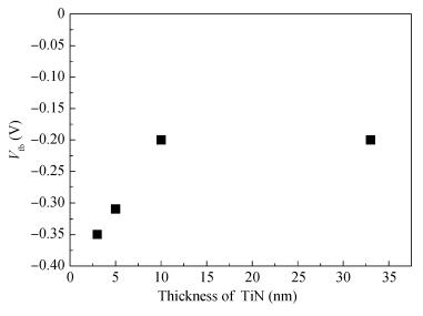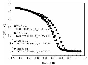
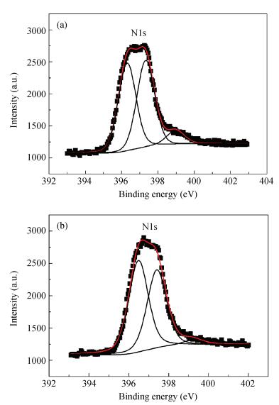
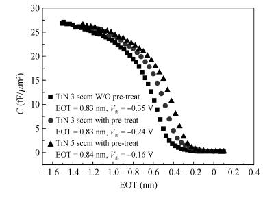
Fig. 1.
The $C$ –$V$ characteristics for capacitors with different thicknesses of TiN.
SEMICONDUCTOR TECHNOLOGY
Kai Han, Xueli Ma, Hong Yang and Wenwu Wang
Corresponding author: Han Kai, Email:hankai@ime.ac.cn
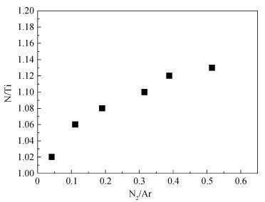
Abstract: It is important to find a way to modulate the work function of TiN metal gate towards the valence band edge of Si, which can meet the lower threshold voltage requirement of p-type metal-oxide-semiconductor (MOS) transistor. In this work, effects of TiN thickness, post-deposition annealing (PDA), oxygen incorporation and N concentration variation on the work function of TiN metal gate in MOS structures are systematically investigated. It can be found that the work function positively shifts at the initial stage as the thickness of the TiN layer increases and stabilizes at such a thickness. PDA at N2 ambience with a trace of O2 can also cause a positive shift in the work function of TiN metal gate. The same tendency can be observed when oxygen is incorporated into TiN. Finally, increasing the N concentration in TiN can also positively shift the work function. All these measures are effective in modulating the TiN metal gate so that it is more suitable for PMOS application.
Keywords: work function modulation, PMOS, positive shift
| [1] |
Wilk G D, Wallace R M, Anthony J M. high-k gate dielectrics:current status and materials properties considerations. J Appl Phys, 2001, 89(10):5243 doi: 10.1063/1.1361065
|
| [2] |
Zhao Y, Toyama M, Kita K, et al. Moisture-absorption-induced permittivity deterioration and surface roughness enhancement of lanthanum oxide films on silicon. Appl Phys Lett, 2006, 88(7):072904 doi: 10.1063/1.2174840
|
| [3] |
Chau R, Brask J, Datta S, et al. Application of high-k gate dielectrics and metal gate electrodes to enable silicon and non-silicon logic nanotechnology. Microelectron Eng, 2005, 80:1 doi: 10.1016/j.mee.2005.04.035
|
| [4] |
Narayanan V, Paruchuri V K, Bojarczuk N A, et al. Band-edge high-performance high-k/metal gate n-MOSFETs using cap layers containing group ⅡA and ⅢB elements with gate-first processing for 45 nm and beyond. Dig Tech Pap Symp VLSI Technol, 2006:224
|
| [5] |
Kadoshima M, Matsuki T, Miyazaki S, et al. Effective-work-function control by barying the TiN thickness in poly-Si/TiN gate electrodes for scaled high-k CMOSFETs. IEEE Electron Device Lett, 2009, 30(5):466 doi: 10.1109/LED.2009.2016585
|
| [6] |
Westlinder J, Sjöblom G, Olsson J. Variable work function in MOS capacitors utilizing nitrogen-controlled TiNx gate electrodes. Microelectron Eng, 2004, 75:389 doi: 10.1016/j.mee.2004.07.061
|
| [7] |
Mistry K, Allen C, Auth C, et al. A 45 nm logic technology with high-k+metal gate transistors, strained silicon, 9 Cu interconnect layers, 193 nm dry patterning, and 100% Pb-free packaging. Tech Dig Int Electron Devices Meeting, 2007:247
|
| [8] |
Bai W P, Bae S H, Wen H C, et al. Three-layer laminated metal gate electrodes with tunable work functions for CMOS applications. IEEE Electron Device Lett, 2005, 26(4):231 doi: 10.1109/LED.2005.844701
|
| [9] |
Choi C H, Lee K L, Narayanan V. Impact of diffusionless anneal using dynamic surface anneal on the electrical properties of a high-k/metal gate stack in metal-oxide-semiconductor devices. Appl Phys Lett, 2011, 98(12):123506 doi: 10.1063/1.3570655
|
| [10] |
Li Z L, Schram T, Witters T, et al. Oxygen incorporation in TiN for metal gate work function tuning with a replacement gate integration approach. Microelectron Eng, 2010, 87:1805 doi: 10.1016/j.mee.2009.10.023
|


Article views: 4875 Times PDF downloads: 253 Times Cited by: 0 Times
Received: 03 November 2012 Revised: 13 February 2013 Online: Published: 01 August 2013
| Citation: |
Kai Han, Xueli Ma, Hong Yang, Wenwu Wang. Modulation of the effective work function of TiN metal gate for PMOS application[J]. Journal of Semiconductors, 2013, 34(8): 086002. doi: 10.1088/1674-4926/34/8/086002
****
K Han, X L Ma, H Yang, W W Wang. Modulation of the effective work function of TiN metal gate for PMOS application[J]. J. Semicond., 2013, 34(8): 086002. doi: 10.1088/1674-4926/34/8/086002.

|
| [1] |
Wilk G D, Wallace R M, Anthony J M. high-k gate dielectrics:current status and materials properties considerations. J Appl Phys, 2001, 89(10):5243 doi: 10.1063/1.1361065
|
| [2] |
Zhao Y, Toyama M, Kita K, et al. Moisture-absorption-induced permittivity deterioration and surface roughness enhancement of lanthanum oxide films on silicon. Appl Phys Lett, 2006, 88(7):072904 doi: 10.1063/1.2174840
|
| [3] |
Chau R, Brask J, Datta S, et al. Application of high-k gate dielectrics and metal gate electrodes to enable silicon and non-silicon logic nanotechnology. Microelectron Eng, 2005, 80:1 doi: 10.1016/j.mee.2005.04.035
|
| [4] |
Narayanan V, Paruchuri V K, Bojarczuk N A, et al. Band-edge high-performance high-k/metal gate n-MOSFETs using cap layers containing group ⅡA and ⅢB elements with gate-first processing for 45 nm and beyond. Dig Tech Pap Symp VLSI Technol, 2006:224
|
| [5] |
Kadoshima M, Matsuki T, Miyazaki S, et al. Effective-work-function control by barying the TiN thickness in poly-Si/TiN gate electrodes for scaled high-k CMOSFETs. IEEE Electron Device Lett, 2009, 30(5):466 doi: 10.1109/LED.2009.2016585
|
| [6] |
Westlinder J, Sjöblom G, Olsson J. Variable work function in MOS capacitors utilizing nitrogen-controlled TiNx gate electrodes. Microelectron Eng, 2004, 75:389 doi: 10.1016/j.mee.2004.07.061
|
| [7] |
Mistry K, Allen C, Auth C, et al. A 45 nm logic technology with high-k+metal gate transistors, strained silicon, 9 Cu interconnect layers, 193 nm dry patterning, and 100% Pb-free packaging. Tech Dig Int Electron Devices Meeting, 2007:247
|
| [8] |
Bai W P, Bae S H, Wen H C, et al. Three-layer laminated metal gate electrodes with tunable work functions for CMOS applications. IEEE Electron Device Lett, 2005, 26(4):231 doi: 10.1109/LED.2005.844701
|
| [9] |
Choi C H, Lee K L, Narayanan V. Impact of diffusionless anneal using dynamic surface anneal on the electrical properties of a high-k/metal gate stack in metal-oxide-semiconductor devices. Appl Phys Lett, 2011, 98(12):123506 doi: 10.1063/1.3570655
|
| [10] |
Li Z L, Schram T, Witters T, et al. Oxygen incorporation in TiN for metal gate work function tuning with a replacement gate integration approach. Microelectron Eng, 2010, 87:1805 doi: 10.1016/j.mee.2009.10.023
|

 WeChat ID
Journal of Semiconductors © 2017 All Rights Reserved 京ICP备05085259号-2

 DownLoad: