| Citation: |
Yongheng Jiang, Xiaorong Luo, Yanfei Li, Pei Wang, Ye Fan, Kun Zhou, Qi Wang, Xiarong Hu, Bo Zhang. Eliminating the floating-body effects in a novel CMOS-compatible thin-SOI LDMOS[J]. Journal of Semiconductors, 2013, 34(9): 094005. doi: 10.1088/1674-4926/34/9/094005
****
Y H Jiang, X R Luo, Y F Li, P Wang, Y Fan, K Zhou, Q Wang, X R Hu, B Zhang. Eliminating the floating-body effects in a novel CMOS-compatible thin-SOI LDMOS[J]. J. Semicond., 2013, 34(9): 094005. doi: 10.1088/1674-4926/34/9/094005.
|
Eliminating the floating-body effects in a novel CMOS-compatible thin-SOI LDMOS
DOI: 10.1088/1674-4926/34/9/094005
More Information
-
Abstract
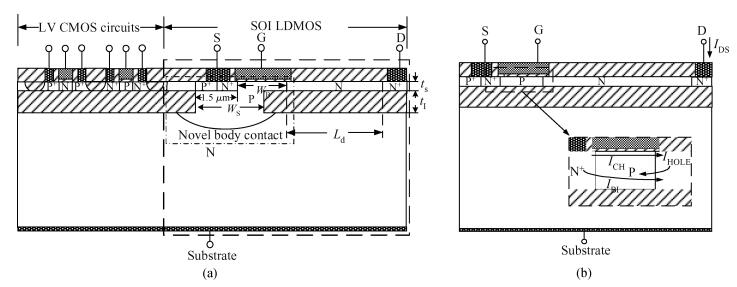
A novel CMOS-compatible thin film SOI LDMOS with a novel body contact structure is proposed. It has a Si window and a P-body extended to the substrate through the Si window, thus, the P-body touches the P+ region to form the body contact. Compared with the conventional floating body SOI LDMOS (FB SOI LDMOS) structure, the new structure increases the off-state BV by 54%, decreases the specific on resistance by 20%, improves the output characteristics significantly, and suppresses the self-heating effect. Furthermore, the advantages of the low leakage current and low output capacitance of SOI devices do not degrade. -
References
[1] Colinge J P. Silicon-on-insulator technology:materials to VLSI, 2nd ed. Netherlands:Kluwer Academic Publisher, 1997:123[2] Xue S B, Huang R, Huang D T, et al. Impact of the displacement damage in channel and source/drain regions on the DC characteristics degradation in deep-submicron MOSFETs after heavy ion irradiation. Chin Phys B, 2010, 19(11):117307 doi: 10.1088/1674-1056/19/11/117307[3] Choi J Y, Fossum J G. Analysis and control of floating-body bipolar effects in fully depleted submicrometer SOI MOSFET's. IEEE Trans Electron Devices, 1991, 38(6):1384 doi: 10.1109/16.81630[4] Eric P Ver P, Cuong T N, Simon W S, et al. Parasitic bipolar gain in fully depleted n-channel SOI MOSFET's. IEEE Trans Electron Devices, 1994, 41(6):970 doi: 10.1109/16.293310[5] Chen C E D, Mishel M, Sundaresan R, et al. Single-transistor latch in SOI MOSFET's. IEEE Electron Device Lett, 1988, 9(12):636 doi: 10.1109/55.20420[6] Liu Y L, Liu X Y, Han Z S, et al. Simulation of a novel Schottky body-contacted structure suppressing floating body effect in partially-depleted SOI nMOSFET's. Chinese Journal of Semiconductors, 2002, 23(10):1019[7] Cheng X H, Yang W W, Song Z R, et al. A novel LDMOS structure in thin film patterned-SOI technology with a silicon window beneath p well. Chinese Journal of Semiconductors, 2004, 25(12):1581[8] Sleight J, Mistry K. A compact Schottky body contact technology for SOI transistors. International Electron Devices Meeting, Washington, DC, USA, 1997:419[9] Min B W, Wu L K D, Caffo D, et al. Reduction of hysterestic propagation delay with less performance degradation by novel body contact in PD SOI application. IEEE International SOI Conference, Williamsburg, USA, 2002:169[10] Zhou J H, Gao M H, Pang S K, et al. Body-contact self-bias effect in partially depleted SOI-CMOS and alternatives to suppress floating body effect. Journal of Semiconductors, 2011, 32(2):024003 doi: 10.1088/1674-4926/32/2/024003[11] Liu Y L, Liu X Y, Han Z S, et al. Floating body effect in partially depleted SOI nMOSFET with asymmetric structure and Ge-implantation. Chinese Journal of Semiconductors, 2002, 23(11):1154[12] Cai X W, Hai C H. Study of body contact of partial depleted SOI NMOS devices. 8th International Conference on Solid-State and Integrated Circuit Technology, Shanghai, China, 2006:212[13] Hai C H, Han Z S, Zhao L X, et al. Study of improved performance of SOI devices and circuits. Chinese Journal of Semiconductors, 2006, 27:322[14] Daghighi A, Osman M A. Three-dimensional simulation of body contact structures in PD SOI MOSFETs. Proceedings of the 15th Biennial University/Government/Industry Microelectronics Symposium, Boise, USA, 2003:288[15] Merchant S, Arnold E, Baumgart S, et al. Realization of high breakdown voltage (> 700 V) in thin SOI devices. Proceedings of the 3rd International Symposium on Power Semiconductor Devices and ICs, Baltimore, USA, 1991:31[16] Baliga B J. Power semiconductor devices. Boston:MA PWS, 1996:155[17] Bi J S, Song L M, Hai C H, et al. Back-gate effect of SOI LDMOSFETs. Journal of Semiconductors, 2008, 29(11):2148 http://www.jos.ac.cn/bdtxben/ch/reader/view_abstract.aspx?file_no=08032508&flag=1 -
Proportional views


 DownLoad:

