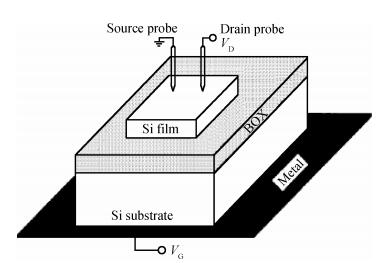
Fig. 1.
Structure of the traditional pseudo-MOS
SEMICONDUCTOR DEVICES
Shiyao Liu1, , Wei He1, Jianmin Cao1 and Siwen Huang1
Corresponding author: Liu Shiyao, Email:lewis_yao@163.com
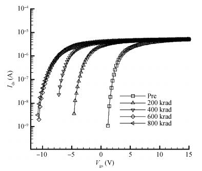
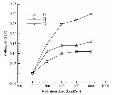
Abstract: This paper investigates the total ionizing dose response of different non-planar triple-gate transistor structures with different fin widths. By exposing the pseudo-MOS transistor to different amounts of radiation, different interface trap densities and trapped-oxide charges can be obtained. Using these parameters together with Altal 3D simulation software, the total dose radiation response of various non-planar triple-gate devices can be simulated. The behaviors of three kinds of non-planar devices are compared.
Keywords: silicon-on-insulator, total ionizing dose effects, pseudo-MOS, non-planar triple-gate transistors
| [1] |
Rashkeev S N, Cirba C R, Fleetwood D M, et al. Physical model for enhanced interface-trap formation at low dose rates. IEEE Trans Nucl Sci, 2002, 49(6):26505 http://ieeexplore.ieee.org/document/1134199/authors
|
| [2] |
Chen X J, Barnaby H J, Vermeire B, et al. Mechanisms of enhanced radiation induced degradation due to excess molecular hydrogen in bipolar oxides. IEEE Trans Nucl Sci, 2007, 54(6):1993
|
| [3] |
Hjalmarson H P, Pease R L, Witczak S C, et al. Mechanisms for radiation dose-rate sensitivity of bipolar transistors. IEEE Trans Nucl Sci, 2003, 50(6):1901 doi: 10.1109/TNS.2003.821803
|
| [4] |
Wang T Q, Wei X D, Li H J, et al. Calculation of X-ray attenuation and energy deposition. Atomic Energy Science and Technology, 2007, 41(4):399(in Chinese)
|
| [5] |
Scofield J H, Fleetwood D M. Physical basis for nondestructive tests of MOS radiation hardness. IEEE Trans Nucl Sci, 1991, 38(6):1567 doi: 10.1109/23.124147
|
| [6] |
Yoshino A, Ma T P, Okumura K. Front-and back-interface trap densities and subthreshold swings of fully depleted mode metal-oxide-semiconductor transistors fabricated on separation-by-implanted-oxygen substrates. Jpn J Appl Phys, 1998, 37(7):3933
|
| [7] |
Gaillardin M, Paillet P, Ferlet-Cavrois V, et al. High tolerance to total ionizing dose of Ω -shaped gate field-effect transistors. Appl Phys Lett, 2006, 88(22):223511 doi: 10.1063/1.2206097
|
| [8] |
Gaillardin M, Paillet P, Ferlet-Cavrois V, et al. Total ionizing dose effects on triple-gate FETs. IEEE Trans Nucl Sci, 2006, 53(6):3158 doi: 10.1109/TNS.2006.884351
|
| [9] |
Daugé F, Pretet J, Cristoloveanu S, et al. Coupling effects and channels separation in FinFETs. Solid-State Electron, 2004, 48(4):535 doi: 10.1016/j.sse.2003.09.033
|
| [10] |
Ritzenthaler R, Cristoloveanu S, Faynot O, et al. Lateral coupling and immunity to substrate effect in FET devices. Solid State Electron, 2006, 50(3):558
|


Article views: 3385 Times PDF downloads: 14 Times Cited by: 0 Times
Received: 25 December 2012 Revised: 23 April 2013 Online: Published: 01 September 2013
| Citation: |
Shiyao Liu, Wei He, Jianmin Cao, Siwen Huang. The total ionizing dose effects of non-planar triple-gate transistors[J]. Journal of Semiconductors, 2013, 34(9): 094004. doi: 10.1088/1674-4926/34/9/094004
****
S Y Liu, W He, J M Cao, S W Huang. The total ionizing dose effects of non-planar triple-gate transistors[J]. J. Semicond., 2013, 34(9): 094004. doi: 10.1088/1674-4926/34/9/094004.

|
| [1] |
Rashkeev S N, Cirba C R, Fleetwood D M, et al. Physical model for enhanced interface-trap formation at low dose rates. IEEE Trans Nucl Sci, 2002, 49(6):26505 http://ieeexplore.ieee.org/document/1134199/authors
|
| [2] |
Chen X J, Barnaby H J, Vermeire B, et al. Mechanisms of enhanced radiation induced degradation due to excess molecular hydrogen in bipolar oxides. IEEE Trans Nucl Sci, 2007, 54(6):1993
|
| [3] |
Hjalmarson H P, Pease R L, Witczak S C, et al. Mechanisms for radiation dose-rate sensitivity of bipolar transistors. IEEE Trans Nucl Sci, 2003, 50(6):1901 doi: 10.1109/TNS.2003.821803
|
| [4] |
Wang T Q, Wei X D, Li H J, et al. Calculation of X-ray attenuation and energy deposition. Atomic Energy Science and Technology, 2007, 41(4):399(in Chinese)
|
| [5] |
Scofield J H, Fleetwood D M. Physical basis for nondestructive tests of MOS radiation hardness. IEEE Trans Nucl Sci, 1991, 38(6):1567 doi: 10.1109/23.124147
|
| [6] |
Yoshino A, Ma T P, Okumura K. Front-and back-interface trap densities and subthreshold swings of fully depleted mode metal-oxide-semiconductor transistors fabricated on separation-by-implanted-oxygen substrates. Jpn J Appl Phys, 1998, 37(7):3933
|
| [7] |
Gaillardin M, Paillet P, Ferlet-Cavrois V, et al. High tolerance to total ionizing dose of Ω -shaped gate field-effect transistors. Appl Phys Lett, 2006, 88(22):223511 doi: 10.1063/1.2206097
|
| [8] |
Gaillardin M, Paillet P, Ferlet-Cavrois V, et al. Total ionizing dose effects on triple-gate FETs. IEEE Trans Nucl Sci, 2006, 53(6):3158 doi: 10.1109/TNS.2006.884351
|
| [9] |
Daugé F, Pretet J, Cristoloveanu S, et al. Coupling effects and channels separation in FinFETs. Solid-State Electron, 2004, 48(4):535 doi: 10.1016/j.sse.2003.09.033
|
| [10] |
Ritzenthaler R, Cristoloveanu S, Faynot O, et al. Lateral coupling and immunity to substrate effect in FET devices. Solid State Electron, 2006, 50(3):558
|

 WeChat ID
Journal of Semiconductors © 2017 All Rights Reserved 京ICP备05085259号-2

 DownLoad: