


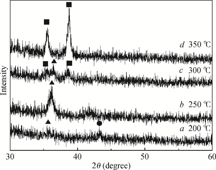
Fig. 1.
X-ray diffraction patterns of copper oxide films oxidized at different temperatures. (Symbol representations: Cu-solid round; Cu2Osolid triangle; CuO-solid square)
SEMICONDUCTOR MATERIALS
Ping Zhang1, Yurong Zhou1, , Qingbo Yan1, Fengzhen Liu1, Jingwen Li2 and Gangqiang Dong1
Corresponding author: Zhou Yurong, Email:zhouyurong@ucas.ac.cn
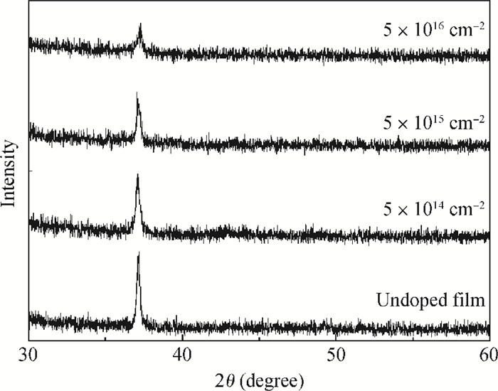
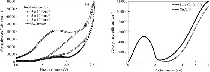
Abstract: Highly-oriented Cu2O thin films were prepared by low temperature thermal oxidation of evaporated Cu thin films. The films were doped with different doses of nitrogen by ion implantation. An absorption peak appears below the absorption edge in the absorption spectrum of highly nitrogen doped Cu2O. The effect of nitrogen doping on the crystal structure, electronic structure and optical properties of Cu2O were investigated systematically by first-principles calculations. The calculation results indicate that an intermediate energy band exists in the forbidden gap of highly nitrogen doped Cu2O. The electron transition from the valence band to the intermediate band is consistent with the absorption peak by experimental observation. Experimental and computational results indicate that nitrogen doped Cu2O could be a suitable absorbing material candidate for wide-spectrum detectors or intermediate band solar cells.
Keywords: cuprous oxide, ion implantation, nitrogen doping, intermediate band, first-principles calculations
| [1] |
Luque A, Marti A. Increasing the efficiency of ideal solar cells by photon induced transitions at intermediate levels. Phys Rev Lett, 1997, 78(26):5014. doi: 10.1103/PhysRevLett.78.5014
|
| [2] |
Jeong S, Aydil E S. Heteroepitaxial growth of Cu2O thin film on ZnO by metal organic chemical vapor deposition. J Cryst Growth, 2009, 311(17):4188 doi: 10.1016/j.jcrysgro.2009.07.020
|
| [3] |
Nakaoka K, Ogura K. Electrochemical preparation of p-type cupric and cuprous oxides on platinum and gold substrates from copper(Ⅱ) solutions with various amino acids. J Electrochem Soc, 2002, 149(11):579 doi: 10.1149/1.1512670
|
| [4] |
Papadimitropoulos G, Vourdas N, Em V V, et al. Optical and structural properties of copper oxide thin films grown by oxidation of metal layers. Thin Solid Films. 2006, 515(4):2428 doi: 10.1016/j.tsf.2006.06.002
|
| [5] |
Lee Y S, Winkler M T, Siah S C, et al. Hall mobility of cuprous oxide thin films deposited by reactive direct-current magnetron sputtering. Appl Phys Lett, 2011, 98:192115 doi: 10.1063/1.3589810
|
| [6] |
Zhu H L, Zhang J Y, Li C Z, et al. Cu2O thin films deposited by reactive direct current magnetron sputtering. Thin Solid Films, 2009, 517:5700 doi: 10.1016/j.tsf.2009.02.127
|
| [7] |
Grondahl L O, Geiger P H. A new electronic rectifier. Journal of the American Institute of Electrical Engineers, 1927, 46:215
|
| [8] |
Ghisjen J, Tjeng L H, van Elp J, et al. Electronic structure of Cu2O and CuO. Phys Rev B, 1988, 38(16):11322 doi: 10.1103/PhysRevB.38.11322
|
| [9] |
Malerba C, Azanza Ricardo C L, D'Incau M, et al. Nitrogen doped Cu2O:a possible material for intermediate band solar cells. Solar Energy Materials & Solar Cells, 2012, 105:192
|
| [10] |
Figueiredo V, Elangovan E, Goncalves G, et al. Effect of post-annealing on the properties of copper oxide thin films obtained from the oxidation of evaporated metallic copper. Appl Surf Sci, 2008, 254:3949 doi: 10.1016/j.apsusc.2007.12.019
|
| [11] |
Gevorkyan V A, Reymers A E, Nersesyan M N, et al. Characterization of Cu2O thin films prepared by evaporation of CuO powder. J Phys:Conference Series, 2012, 350:012027 doi: 10.1088/1742-6596/350/1/012027
|
| [12] |
Clark S J, Segall M D, Pickard C J, et al. M. First principles methods Using CASTEP. Z Kristallogr, 2005, 220:567
|
| [13] |
Perdew J P, Burke K, Ernzerhof M. Generalized gradient approximation made simple. Phys Rev Lett, 1996, 77:3865 doi: 10.1103/PhysRevLett.77.3865
|
| [14] |
Vanderbilt D. Soft self-consistent pseudopotentials in a generalized eigenvalue formalism. Phys Rev B, 1990, 41:7892 doi: 10.1103/PhysRevB.41.7892
|
| [15] |
Monkhorst H J, Pack J D. Special points for Brillouin-zone integrations. Phys Rev B, 1976, 13(12):5188 doi: 10.1103/PhysRevB.13.5188
|
| [16] |
Pfrommer B G, Câté M, Louie S G, et al. Relaxation of crystals with the quasi-Newton method. J Comput Phys, 1997, 131:233 doi: 10.1006/jcph.1996.5612
|
| [17] |
Plata J J, Márquez A M, Sanz J F. Communication:Improving the density functional theory +U description of CeO2 by including the contribution of the O 2P electrons. J Chem Phys, 2012, 136(4):1101
|
| [18] |
Wang Qixin, Xiong Zhihua, Rao Jianping, et al. First-principles calculation of ZnO doped with Ag. Chinese Journal of Semiconductors, 2007, 28(5):696(in Chinese)
|
| [19] |
Sheetz R M, Ponomareva I, Richter E, et al. Defect-induced optical absorption in the visible range in ZnO nanowires. Phys Rev B, 2009, 80:195314 doi: 10.1103/PhysRevB.80.195314
|
| [20] |
Campo Jr V L, Cococcioni M. Extended DFT + U + V method with on-site and inter-site electronic interactions. J Phys:Condens Matter, 2010, 22:055602 doi: 10.1088/0953-8984/22/5/055602
|
| [21] |
Park S G, Magyari-Köpe B, Nishi Y. Electronic correlation effects in reduced rutile TiO2 within the LDA + U method. Phys Rev B, 2010, 82:115109 doi: 10.1103/PhysRevB.82.115109
|
| [22] |
Werner A, Hochheimer H D. High-pressure X-ray study of Cu2O and Ag2O. Phys Rev B, 1982, 25:5929 doi: 10.1103/PhysRevB.25.5929
|
| [23] |
Wang G, Wu S, Geng Z H, et al. First-principles study on the electronic and optical properties of SnxGe1-x. Opt Commun, 2010, 283:4307 doi: 10.1016/j.optcom.2010.06.053
|
| [24] |
Li Jingbo, Wei Suhuai. Alignment of isovalent impurity levels:oxygen impurity in Ⅱ-Ⅵ semiconductors. Phys Rev B, 2006, 73:041201
|
| [25] |
Li J B, Wang L W. Energy levels of isoelectronic impurities by large scale LDA calculations. Phys Rev B, 2003, 67:033102 doi: 10.1103/PhysRevB.67.033102
|


Article views: 3113 Times PDF downloads: 14 Times Cited by: 0 Times
Received: 22 February 2014 Revised: 27 March 2014 Online: Published: 01 October 2014
| Citation: |
Ping Zhang, Yurong Zhou, Qingbo Yan, Fengzhen Liu, Jingwen Li, Gangqiang Dong. A combined experimental-computational study on nitrogen doped Cu2O as the wide-spectrum absorption material[J]. Journal of Semiconductors, 2014, 35(10): 103001. doi: 10.1088/1674-4926/35/10/103001
****
P Zhang, Y R Zhou, Q B Yan, F Z Liu, J W Li, G Q Dong. A combined experimental-computational study on nitrogen doped Cu2O as the wide-spectrum absorption material[J]. J. Semicond., 2014, 35(10): 103001. doi: 10.1088/1674-4926/35/10/103001.

|
| [1] |
Luque A, Marti A. Increasing the efficiency of ideal solar cells by photon induced transitions at intermediate levels. Phys Rev Lett, 1997, 78(26):5014. doi: 10.1103/PhysRevLett.78.5014
|
| [2] |
Jeong S, Aydil E S. Heteroepitaxial growth of Cu2O thin film on ZnO by metal organic chemical vapor deposition. J Cryst Growth, 2009, 311(17):4188 doi: 10.1016/j.jcrysgro.2009.07.020
|
| [3] |
Nakaoka K, Ogura K. Electrochemical preparation of p-type cupric and cuprous oxides on platinum and gold substrates from copper(Ⅱ) solutions with various amino acids. J Electrochem Soc, 2002, 149(11):579 doi: 10.1149/1.1512670
|
| [4] |
Papadimitropoulos G, Vourdas N, Em V V, et al. Optical and structural properties of copper oxide thin films grown by oxidation of metal layers. Thin Solid Films. 2006, 515(4):2428 doi: 10.1016/j.tsf.2006.06.002
|
| [5] |
Lee Y S, Winkler M T, Siah S C, et al. Hall mobility of cuprous oxide thin films deposited by reactive direct-current magnetron sputtering. Appl Phys Lett, 2011, 98:192115 doi: 10.1063/1.3589810
|
| [6] |
Zhu H L, Zhang J Y, Li C Z, et al. Cu2O thin films deposited by reactive direct current magnetron sputtering. Thin Solid Films, 2009, 517:5700 doi: 10.1016/j.tsf.2009.02.127
|
| [7] |
Grondahl L O, Geiger P H. A new electronic rectifier. Journal of the American Institute of Electrical Engineers, 1927, 46:215
|
| [8] |
Ghisjen J, Tjeng L H, van Elp J, et al. Electronic structure of Cu2O and CuO. Phys Rev B, 1988, 38(16):11322 doi: 10.1103/PhysRevB.38.11322
|
| [9] |
Malerba C, Azanza Ricardo C L, D'Incau M, et al. Nitrogen doped Cu2O:a possible material for intermediate band solar cells. Solar Energy Materials & Solar Cells, 2012, 105:192
|
| [10] |
Figueiredo V, Elangovan E, Goncalves G, et al. Effect of post-annealing on the properties of copper oxide thin films obtained from the oxidation of evaporated metallic copper. Appl Surf Sci, 2008, 254:3949 doi: 10.1016/j.apsusc.2007.12.019
|
| [11] |
Gevorkyan V A, Reymers A E, Nersesyan M N, et al. Characterization of Cu2O thin films prepared by evaporation of CuO powder. J Phys:Conference Series, 2012, 350:012027 doi: 10.1088/1742-6596/350/1/012027
|
| [12] |
Clark S J, Segall M D, Pickard C J, et al. M. First principles methods Using CASTEP. Z Kristallogr, 2005, 220:567
|
| [13] |
Perdew J P, Burke K, Ernzerhof M. Generalized gradient approximation made simple. Phys Rev Lett, 1996, 77:3865 doi: 10.1103/PhysRevLett.77.3865
|
| [14] |
Vanderbilt D. Soft self-consistent pseudopotentials in a generalized eigenvalue formalism. Phys Rev B, 1990, 41:7892 doi: 10.1103/PhysRevB.41.7892
|
| [15] |
Monkhorst H J, Pack J D. Special points for Brillouin-zone integrations. Phys Rev B, 1976, 13(12):5188 doi: 10.1103/PhysRevB.13.5188
|
| [16] |
Pfrommer B G, Câté M, Louie S G, et al. Relaxation of crystals with the quasi-Newton method. J Comput Phys, 1997, 131:233 doi: 10.1006/jcph.1996.5612
|
| [17] |
Plata J J, Márquez A M, Sanz J F. Communication:Improving the density functional theory +U description of CeO2 by including the contribution of the O 2P electrons. J Chem Phys, 2012, 136(4):1101
|
| [18] |
Wang Qixin, Xiong Zhihua, Rao Jianping, et al. First-principles calculation of ZnO doped with Ag. Chinese Journal of Semiconductors, 2007, 28(5):696(in Chinese)
|
| [19] |
Sheetz R M, Ponomareva I, Richter E, et al. Defect-induced optical absorption in the visible range in ZnO nanowires. Phys Rev B, 2009, 80:195314 doi: 10.1103/PhysRevB.80.195314
|
| [20] |
Campo Jr V L, Cococcioni M. Extended DFT + U + V method with on-site and inter-site electronic interactions. J Phys:Condens Matter, 2010, 22:055602 doi: 10.1088/0953-8984/22/5/055602
|
| [21] |
Park S G, Magyari-Köpe B, Nishi Y. Electronic correlation effects in reduced rutile TiO2 within the LDA + U method. Phys Rev B, 2010, 82:115109 doi: 10.1103/PhysRevB.82.115109
|
| [22] |
Werner A, Hochheimer H D. High-pressure X-ray study of Cu2O and Ag2O. Phys Rev B, 1982, 25:5929 doi: 10.1103/PhysRevB.25.5929
|
| [23] |
Wang G, Wu S, Geng Z H, et al. First-principles study on the electronic and optical properties of SnxGe1-x. Opt Commun, 2010, 283:4307 doi: 10.1016/j.optcom.2010.06.053
|
| [24] |
Li Jingbo, Wei Suhuai. Alignment of isovalent impurity levels:oxygen impurity in Ⅱ-Ⅵ semiconductors. Phys Rev B, 2006, 73:041201
|
| [25] |
Li J B, Wang L W. Energy levels of isoelectronic impurities by large scale LDA calculations. Phys Rev B, 2003, 67:033102 doi: 10.1103/PhysRevB.67.033102
|

 WeChat ID
Journal of Semiconductors © 2017 All Rights Reserved 京ICP备05085259号-2

 DownLoad:

