


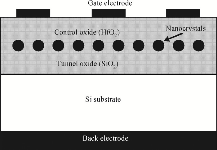
Fig. 1.
Schematic cross-sectional structure of the MOS capacitor using metal NCs embedded between the silica and hafnium oxide layer as charge storage elements.
SEMICONDUCTOR MATERIALS
Peihong Cheng1, 2, Shihua Huang1, and Fang Lu2
Corresponding author: Huang Shihua, Email:huangshihua@zjnu.cn
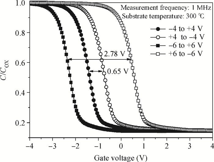
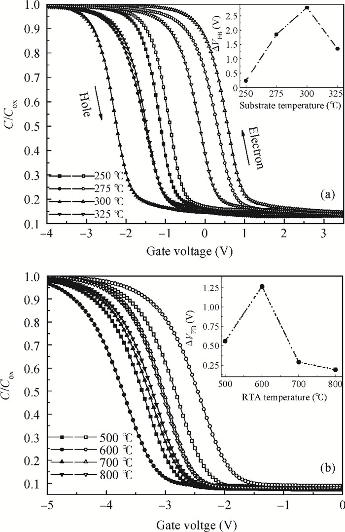
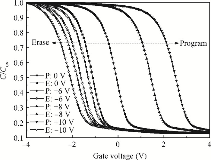
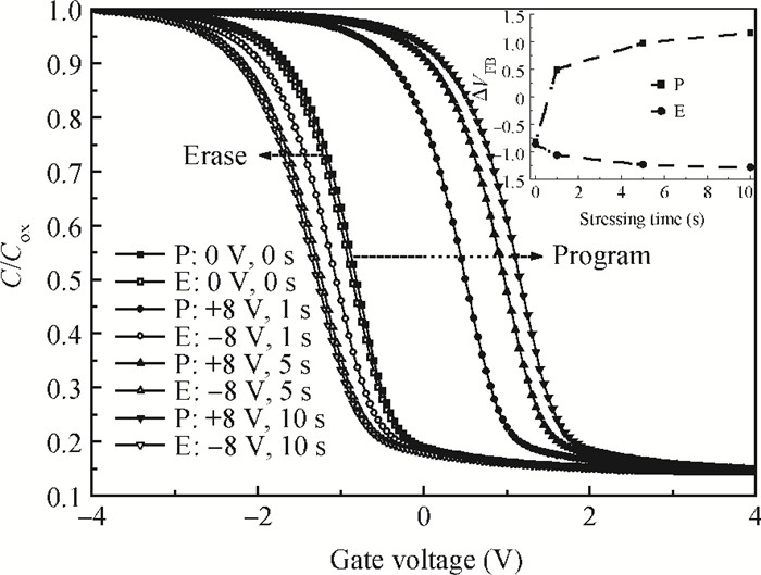
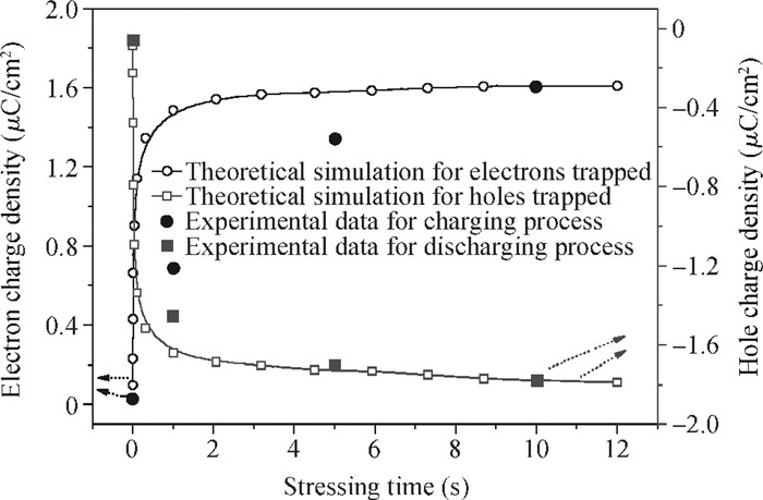
Abstract: The rapid thermal annealing (RTA) nano-crystallization method is widely used in the metal nanocrystal fabrication process. However, the high temperature (usually 600-900℃) in the RTA process will worsen the performance and reliability of devices. A novel method has been proposed to grow metal nanocrystal by synchronous in situ nano-crystallization of metal thin film (SINC), which is able to resolve the problems mentioned above. Compared with Ni nanocrystals (NCs) formed by RTA, Ni NCs prepared by SINC can obtain more energy to crystallize, and its crystallization temperature is greatly reduced. A large memory window (2.78 V) was observed for Ni NCs deposited by SINC at 300℃. However, the largest window is only 1.26 V for Ni NCs formed by RTA at 600℃. A large change (from 0.20 to 4.59 V) of the memory window was observed while the operation voltage increased from 0 to ±10 V, which is due to an occurrence of strong carrier trapping in Ni NCs. Flat-band voltage shift rapidly increases to its saturation value, which indicates that electron/hole trapping in Ni NCs mainly occurs at the initial stage of the program/erase process. A theoretical model was proposed to characterize the charging and discharging processes.
Keywords: metal nanocrystal memory, synchronously crystallization, C-V characteristics
| [1] |
Tiwari S, Rana F, Hanafi H, et al. A silicon nanocrystals based memory. Appl Phys Lett, 1996, 68(10):1377 doi: 10.1063/1.116085
|
| [2] |
Ostraat M L, De Blauwe J W, Green M L, et al. Synthesis and characterization of aerosol silicon nanocrystal nonvolatile floating-gate memory devices. Appl Phys Lett, 2001, 79(3):433 doi: 10.1063/1.1385190
|
| [3] |
Kwon Y H, Park C J, Lee W C, et al. Memory effects related to deep levels in metal-oxide-semiconductor structure with nanocrystalline Si. Appl Phys Lett, 2002, 80(14):2052 doi: 10.1063/1.1467617
|
| [4] |
Liu Z, Lee C, Narayanan V, et al. Metal nanocrystal memories, part Ⅰ:device design and fabrication. IEEE Trans Electron Devices, 2002, 49(9):1606 doi: 10.1109/TED.2002.802617
|
| [5] |
Park B, Cho K, Koo Y S, et al. Memory characteristics of platinum nanoparticle-embedded MOS capacitors. Current Appl Phys, 2009, 9(6):1334 doi: 10.1016/j.cap.2009.02.013
|
| [6] |
Lee D J, Yim S S, Kim K S, et al. Nonvolatile memory characteristics of atomic layer deposited Ru nanocrystals with a SiO2/Al2O3 bilayered tunnel barrier. J Appl Phys, 2010, 107(1):013707 doi: 10.1063/1.3275346
|
| [7] |
Lee J J, Harada Y, Pyun J W, et al. Nickel nanocrystal formation on HfO2 dielectric for nonvolatile memory device applications. Appl Phys Lett, 2005, 86(10):103505 doi: 10.1063/1.1881778
|
| [8] |
Tan Z, Samanta S K, Yoo W J, et al. Self-assembly of Ni nanocrystals on HfO2 and N-assisted Ni confinement for nonvolatile memory application. Appl Phys Lett, 2005, 86(1):013107 doi: 10.1063/1.1846952
|
| [9] |
Sargentis C, Giannakopoulos K, Travlos A, et al. Simple method for the fabrication of a high dielectric constant metal-oxide-semiconductor capacitor embedded with Pt nanoparticles. Appl Phys Lett, 2006, 88(7):073106 doi: 10.1063/1.2174099
|
| [10] |
Carles R, Farcau C, Bonafos C, et al. The synthesis of single layers of Ag nanocrystals by ultra-low-energy ion implantation for large-scale plasmonic structures. Nanotechnology, 2009, 20(35):355305 doi: 10.1088/0957-4484/20/35/355305
|
| [11] |
Hong A J, Liu C C, Wang Y, et al. Metal nanodot memory by self-assembled block copolymer lift-off. Nano Lett, 2010, 10(1):224 doi: 10.1021/nl903340a
|
| [12] |
Zhu C, Huo Z, Xu Z, et al. Performance enhancement of multilevel cell nonvolatile memory by using a bandgap engineered high-k trapping layer. Appl Phys Lett, 2010, 97(25):253503 doi: 10.1063/1.3531559
|
| [13] |
Stathis J H, DiMaria D J. Reliability projection for ultra-thin oxides at low voltage. Int Electron Dev Meeting, San Francisco, CA, 1998:167 http://ieeexplore.ieee.org/document/00746309/
|
| [14] |
Lo S H, Buchanan D A, Taur Y, et al. Modeling and characterization of n+-and p+-polysilicon-gate ultra-thin oxides (21-26 A). VLSI Symp Dig Tech Papers, Piscataway, NJ, 1997:149 http://ieeexplore.ieee.org/document/623742/?arnumber=623742&punumber%3D4913
|
| [15] |
Kang T K, Wang C C, Tsui B Y, et al. Selectivity investigation of HfO2 to oxide using wet etching. Proc Semicond Manuf Technol Workshop, San Francisco, CA, 2004:87
|
| [16] |
Zhao D, Zhu Y, Liu J. Charge storage in a metal-oxide-semiconductor capacitor containing cobalt nanocrystals. Solid State Electron, 2006, 50(6):268 http://cat.inist.fr/?aModele=afficheN&cpsidt=17499477
|
| [17] |
Kwon Y H, Park C J, Lee W C, et al. Memory effects related to deep levels in metal-oxide-semiconductor structure with nanocrystalline Si. Appl Phys Lett, 2002, 80(14):2502 doi: 10.1063/1.1467617
|
| [18] |
Schuegraf K F, Hu C. Hole injection SiO2 breakdown model for very low voltage lifetime extrapolation. IEEE Trans Electron Devices, 1994, 41(5):761 doi: 10.1109/16.285029
|
| [19] |
Lee W C, Hu C. Modeling CMOS tunneling currents through ultrathin gate oxide due to conduction-and valence-band electron and hole tunneling. IEEE Trans Electron Devices, 2001, 48(7):1366 doi: 10.1109/16.930653
|
| [20] |
Sze S M, Kwok K K N. Physics of semiconductor devices. 3rd ed. New Jersey: John Wiley & Sons, 2007: 134
|


Article views: 2642 Times PDF downloads: 23 Times Cited by: 0 Times
Received: 06 April 2014 Revised: 12 May 2014 Online: Published: 01 October 2014
| Citation: |
Peihong Cheng, Shihua Huang, Fang Lu. Charge storage characteristics of Ni nanocrystals formed by synchronous crystallization[J]. Journal of Semiconductors, 2014, 35(10): 103002. doi: 10.1088/1674-4926/35/10/103002
****
P H Cheng, S H Huang, F Lu. Charge storage characteristics of Ni nanocrystals formed by synchronous crystallization[J]. J. Semicond., 2014, 35(10): 103002. doi: 10.1088/1674-4926/35/10/103002.

|
| [1] |
Tiwari S, Rana F, Hanafi H, et al. A silicon nanocrystals based memory. Appl Phys Lett, 1996, 68(10):1377 doi: 10.1063/1.116085
|
| [2] |
Ostraat M L, De Blauwe J W, Green M L, et al. Synthesis and characterization of aerosol silicon nanocrystal nonvolatile floating-gate memory devices. Appl Phys Lett, 2001, 79(3):433 doi: 10.1063/1.1385190
|
| [3] |
Kwon Y H, Park C J, Lee W C, et al. Memory effects related to deep levels in metal-oxide-semiconductor structure with nanocrystalline Si. Appl Phys Lett, 2002, 80(14):2052 doi: 10.1063/1.1467617
|
| [4] |
Liu Z, Lee C, Narayanan V, et al. Metal nanocrystal memories, part Ⅰ:device design and fabrication. IEEE Trans Electron Devices, 2002, 49(9):1606 doi: 10.1109/TED.2002.802617
|
| [5] |
Park B, Cho K, Koo Y S, et al. Memory characteristics of platinum nanoparticle-embedded MOS capacitors. Current Appl Phys, 2009, 9(6):1334 doi: 10.1016/j.cap.2009.02.013
|
| [6] |
Lee D J, Yim S S, Kim K S, et al. Nonvolatile memory characteristics of atomic layer deposited Ru nanocrystals with a SiO2/Al2O3 bilayered tunnel barrier. J Appl Phys, 2010, 107(1):013707 doi: 10.1063/1.3275346
|
| [7] |
Lee J J, Harada Y, Pyun J W, et al. Nickel nanocrystal formation on HfO2 dielectric for nonvolatile memory device applications. Appl Phys Lett, 2005, 86(10):103505 doi: 10.1063/1.1881778
|
| [8] |
Tan Z, Samanta S K, Yoo W J, et al. Self-assembly of Ni nanocrystals on HfO2 and N-assisted Ni confinement for nonvolatile memory application. Appl Phys Lett, 2005, 86(1):013107 doi: 10.1063/1.1846952
|
| [9] |
Sargentis C, Giannakopoulos K, Travlos A, et al. Simple method for the fabrication of a high dielectric constant metal-oxide-semiconductor capacitor embedded with Pt nanoparticles. Appl Phys Lett, 2006, 88(7):073106 doi: 10.1063/1.2174099
|
| [10] |
Carles R, Farcau C, Bonafos C, et al. The synthesis of single layers of Ag nanocrystals by ultra-low-energy ion implantation for large-scale plasmonic structures. Nanotechnology, 2009, 20(35):355305 doi: 10.1088/0957-4484/20/35/355305
|
| [11] |
Hong A J, Liu C C, Wang Y, et al. Metal nanodot memory by self-assembled block copolymer lift-off. Nano Lett, 2010, 10(1):224 doi: 10.1021/nl903340a
|
| [12] |
Zhu C, Huo Z, Xu Z, et al. Performance enhancement of multilevel cell nonvolatile memory by using a bandgap engineered high-k trapping layer. Appl Phys Lett, 2010, 97(25):253503 doi: 10.1063/1.3531559
|
| [13] |
Stathis J H, DiMaria D J. Reliability projection for ultra-thin oxides at low voltage. Int Electron Dev Meeting, San Francisco, CA, 1998:167 http://ieeexplore.ieee.org/document/00746309/
|
| [14] |
Lo S H, Buchanan D A, Taur Y, et al. Modeling and characterization of n+-and p+-polysilicon-gate ultra-thin oxides (21-26 A). VLSI Symp Dig Tech Papers, Piscataway, NJ, 1997:149 http://ieeexplore.ieee.org/document/623742/?arnumber=623742&punumber%3D4913
|
| [15] |
Kang T K, Wang C C, Tsui B Y, et al. Selectivity investigation of HfO2 to oxide using wet etching. Proc Semicond Manuf Technol Workshop, San Francisco, CA, 2004:87
|
| [16] |
Zhao D, Zhu Y, Liu J. Charge storage in a metal-oxide-semiconductor capacitor containing cobalt nanocrystals. Solid State Electron, 2006, 50(6):268 http://cat.inist.fr/?aModele=afficheN&cpsidt=17499477
|
| [17] |
Kwon Y H, Park C J, Lee W C, et al. Memory effects related to deep levels in metal-oxide-semiconductor structure with nanocrystalline Si. Appl Phys Lett, 2002, 80(14):2502 doi: 10.1063/1.1467617
|
| [18] |
Schuegraf K F, Hu C. Hole injection SiO2 breakdown model for very low voltage lifetime extrapolation. IEEE Trans Electron Devices, 1994, 41(5):761 doi: 10.1109/16.285029
|
| [19] |
Lee W C, Hu C. Modeling CMOS tunneling currents through ultrathin gate oxide due to conduction-and valence-band electron and hole tunneling. IEEE Trans Electron Devices, 2001, 48(7):1366 doi: 10.1109/16.930653
|
| [20] |
Sze S M, Kwok K K N. Physics of semiconductor devices. 3rd ed. New Jersey: John Wiley & Sons, 2007: 134
|

 WeChat ID
Journal of Semiconductors © 2017 All Rights Reserved 京ICP备05085259号-2

 DownLoad:

