


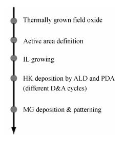
Fig. 1.
Device fabrication process flow
SEMICONDUCTOR TECHNOLOGY
ShuXiang Zhang, Hong Yang, Bo Tang, Zhaoyun Tang, Yefeng Xu, Jing Xu and Jiang Yan
Corresponding author: Yan Jiang, Email:yanjiang@ime.ac.cn
Abstract: ALD HfO2 films fabricated by a novel multi deposition multi annealing (MDMA) technique are investigated, we have included samples both with and without a Ti scavenging layer. As compared to the reference gate stack treated by conventional one-time deposition and annealing (D & A), devices receiving MDMA show a significant reduction in leakage current. Meanwhile, EOT growth is effectively controlled by the Ti scavenging layer. This improvement strongly correlates with the cycle number of D & A (while keeping the total annealing time and total dielectrics thickness the same). Transmission electron microscope and energy-dispersive X-ray spectroscopy analysis suggests that oxygen incorporation into both the high-k film and the interfacial layer is likely to be responsible for the improvement of the device. This novel MDMA is promising for the development of gate stack technology in a gate last integration scheme.
Keywords: postdeposition annealing, scavenging, oxygen vacancy, equivalent oxide thickness, metal gate, high-k
| [1] |
Wen H C, Harris H R, Young C D, et al. On oxygen deficiency and fast transient charge-trapping effects in high-k dielectrics. Electron Device Lett, 2006, 27(12):984 doi: 10.1109/LED.2006.886711
|
| [2] |
Noor F A, Abdullah M. Comparison of electron transmittances and tunneling currents in an anisotropic TiNx/HfO2/SiO2/p-Si(100) metal-oxide-semiconductor (MOS) capacitor calculated using exponential-and Airy-wavefunction approaches and a transfer matrix method. Journal of Semiconductors, 2010, 31(12):124002 doi: 10.1088/1674-4926/31/12/124002
|
| [3] |
Veloso A, Ragnarsson L A, Cho M J, et al. Gate-last vs gate-first technology for aggressively scaled EOT logic/RF CMOS. IEEE Symp VLSI Technol, 2011:34
|
| [4] |
Chen Y T, Fu S I, Chiang W T, et al. Chemical oxide interfacial layer for the high-k-last/gate-last integration scheme. Electron Device Lett, 2012, 33(7):946 doi: 10.1109/LED.2012.2195292
|
| [5] |
Umezawa N, Shiraishi K, Sugino S, et al. Suppression of oxygen vacancy formation in Hf-based high-k dielectrics by lanthanum incorporation. Appl Phys Lett, 2007, 91(13):132904 doi: 10.1063/1.2789392
|
| [6] |
Cartier E, Hopstaken M, Copel M. Oxygen passivation of vacancy defects in metal-nitride gated HfO2/SiO2/Si devices. Appl Phys Lett, 2009, 95(4):042901 doi: 10.1063/1.3186075
|
| [7] |
Yan Z, Ran J. Effect of annealing on characteristics of a HfOxNy-HfO2-HfOxNy sandwich stack compared with HfO2 film. Journal of Semiconductors, 2009, 30(8):082004 doi: 10.1088/1674-4926/30/8/082004
|
| [8] |
Nabatame T, Iwamoto K, Ota H, et al. Design and proof of high quality HfAlOx film formation for MOSCAPs and nMOSFETs through layer-by-layer deposition and annealing process. IEEE Symp VLSI Technol, 2003:25
|
| [9] |
Kim Y H, Cabral C, Gusev E P, et al. Systematic study of work function engineering and scavenging effect using NiSi alloy FuSi metal gates with advanced gate stacks. Electron Devices Meeting (IEDM), 2005:645
|
| [10] |
Wu L, Yu H Y, Li X, et al. Thermal stability of TiN metal gate prepared by atomic layer deposition or physical vapor deposition on HfO2 high-k dielectric. Appl Phys Lett, 2010, 96(11):113510 doi: 10.1063/1.3365241
|
| [11] |
Callegari A, Jamison P, Neumayer D, et al. Electron mobility dependence on annealing temperature of W/HfO gate stacks:the role of the interfacial layer. J Appl Phys, 2006, 99:023709 doi: 10.1063/1.2163980
|
| [12] |
Kim I, Kuk S, Kim S, et al. Thermodynamic properties and interfacial layer characteristics of HfO thin films deposited by plasma-enhanced atomic layer deposition. Appl Phys Lett, 2007, 90:222101 doi: 10.1063/1.2743749
|
| [13] |
Wang G, Xu Q, Yang T, et al. Application of atomic layer deposition tungsten (ALD W) as gate filling metal for 22 nm and beyond nodes CMOS technology. ECS Journal of Solid State Science and Technology, 2014, 3(4):82 doi: 10.1149/2.015404jss
|
| [14] |
Wu L, Yew K S, Ang D S, et al. A novel multi deposition multi room-temperature annealing technique via ultraviolet-ozone to improve high-k/metal (HfZrO/TiN) gate stack integrity for a gate-last process. Electron Devices Meeting (IEDM), 2010:11.6.1
|
| [15] |
Bersuker G, Park C S, Barnett J, et al. The effect of interfacial layer properties on the performance of Hf-based gate stack devices. J Appl Phys, 2006, 100(9):094108 doi: 10.1063/1.2362905
|
| [16] |
Lin Y S, Puthenkovilakam R, Chang J P, et al. Interfacial properties of ZrO2 on silicon. J Appl Phys, 2003, 93(10):5945 doi: 10.1063/1.1563844
|
| [17] |
Lysaght P S, Barnett J, Bersuker G I, et al. Chemical analysis of HfO/Si (100) film systems exposed to NH thermal processing. J Appl Phys, 2007, 101:024105 doi: 10.1063/1.2422746
|
| [18] |
Heh D, Young C D, Brown G A, et al. Spatial distributions of trapping centers in HfO2/SiO2 gate stacks. Appl Phys Lett, 2006, 88(15):152907 doi: 10.1063/1.2195896
|
| [19] |
Gómez A, Castán H, Garcia H, et al. Interface quality of Sc2O3 and Gd2O3 films based metal-insulator-silicon structures using Al, Pt, and Ti gates:effect of buffer layers and scavenging electrodes. J Vac Sci Technol B:Microelectronics and Nanometer Structures, 2013, 31(1):01A106
|
| [20] |
Choi C, Kang C Y, Rhee S J, et al. Aggressively scaled ultra thin undoped HfO2 gate dielectric (EOT < 0.7 nm) with TaN gate electrode using engineered interface layer. Electron Device Lett, 2005, 26(7):454 doi: 10.1109/LED.2005.851240
|
| [21] |
Choi C, Kang C Y, Rhee S J, et al. Fabrication of TaN-gated ultra-thin MOSFETs (EOT < 1.0 nm) with HfO2 using a novel oxygen scavenging process for sub 65 nm application. IEEE Symp VLSI Technol, 2005:226
|
| [22] |
Schmitz J, Weusthof M H H, Hof A J. Leakage current correction in quasi-static CV measurements. Conference on Microelectronic Test Structures, 2004:179
|
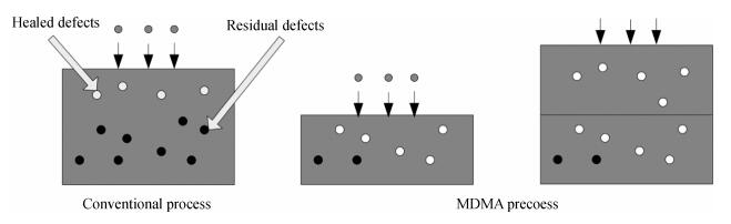
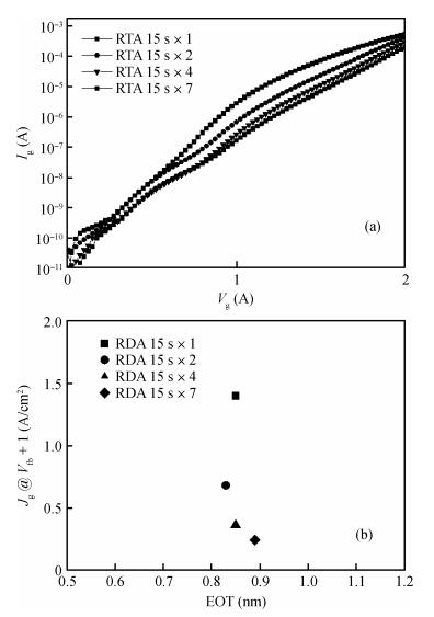
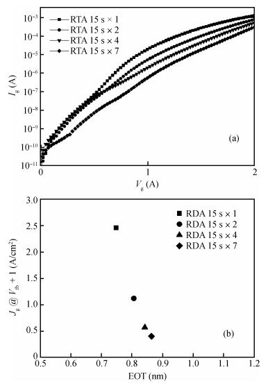
Table 1. The details of HK D & A conditions for all samples

|
| [1] |
Wen H C, Harris H R, Young C D, et al. On oxygen deficiency and fast transient charge-trapping effects in high-k dielectrics. Electron Device Lett, 2006, 27(12):984 doi: 10.1109/LED.2006.886711
|
| [2] |
Noor F A, Abdullah M. Comparison of electron transmittances and tunneling currents in an anisotropic TiNx/HfO2/SiO2/p-Si(100) metal-oxide-semiconductor (MOS) capacitor calculated using exponential-and Airy-wavefunction approaches and a transfer matrix method. Journal of Semiconductors, 2010, 31(12):124002 doi: 10.1088/1674-4926/31/12/124002
|
| [3] |
Veloso A, Ragnarsson L A, Cho M J, et al. Gate-last vs gate-first technology for aggressively scaled EOT logic/RF CMOS. IEEE Symp VLSI Technol, 2011:34
|
| [4] |
Chen Y T, Fu S I, Chiang W T, et al. Chemical oxide interfacial layer for the high-k-last/gate-last integration scheme. Electron Device Lett, 2012, 33(7):946 doi: 10.1109/LED.2012.2195292
|
| [5] |
Umezawa N, Shiraishi K, Sugino S, et al. Suppression of oxygen vacancy formation in Hf-based high-k dielectrics by lanthanum incorporation. Appl Phys Lett, 2007, 91(13):132904 doi: 10.1063/1.2789392
|
| [6] |
Cartier E, Hopstaken M, Copel M. Oxygen passivation of vacancy defects in metal-nitride gated HfO2/SiO2/Si devices. Appl Phys Lett, 2009, 95(4):042901 doi: 10.1063/1.3186075
|
| [7] |
Yan Z, Ran J. Effect of annealing on characteristics of a HfOxNy-HfO2-HfOxNy sandwich stack compared with HfO2 film. Journal of Semiconductors, 2009, 30(8):082004 doi: 10.1088/1674-4926/30/8/082004
|
| [8] |
Nabatame T, Iwamoto K, Ota H, et al. Design and proof of high quality HfAlOx film formation for MOSCAPs and nMOSFETs through layer-by-layer deposition and annealing process. IEEE Symp VLSI Technol, 2003:25
|
| [9] |
Kim Y H, Cabral C, Gusev E P, et al. Systematic study of work function engineering and scavenging effect using NiSi alloy FuSi metal gates with advanced gate stacks. Electron Devices Meeting (IEDM), 2005:645
|
| [10] |
Wu L, Yu H Y, Li X, et al. Thermal stability of TiN metal gate prepared by atomic layer deposition or physical vapor deposition on HfO2 high-k dielectric. Appl Phys Lett, 2010, 96(11):113510 doi: 10.1063/1.3365241
|
| [11] |
Callegari A, Jamison P, Neumayer D, et al. Electron mobility dependence on annealing temperature of W/HfO gate stacks:the role of the interfacial layer. J Appl Phys, 2006, 99:023709 doi: 10.1063/1.2163980
|
| [12] |
Kim I, Kuk S, Kim S, et al. Thermodynamic properties and interfacial layer characteristics of HfO thin films deposited by plasma-enhanced atomic layer deposition. Appl Phys Lett, 2007, 90:222101 doi: 10.1063/1.2743749
|
| [13] |
Wang G, Xu Q, Yang T, et al. Application of atomic layer deposition tungsten (ALD W) as gate filling metal for 22 nm and beyond nodes CMOS technology. ECS Journal of Solid State Science and Technology, 2014, 3(4):82 doi: 10.1149/2.015404jss
|
| [14] |
Wu L, Yew K S, Ang D S, et al. A novel multi deposition multi room-temperature annealing technique via ultraviolet-ozone to improve high-k/metal (HfZrO/TiN) gate stack integrity for a gate-last process. Electron Devices Meeting (IEDM), 2010:11.6.1
|
| [15] |
Bersuker G, Park C S, Barnett J, et al. The effect of interfacial layer properties on the performance of Hf-based gate stack devices. J Appl Phys, 2006, 100(9):094108 doi: 10.1063/1.2362905
|
| [16] |
Lin Y S, Puthenkovilakam R, Chang J P, et al. Interfacial properties of ZrO2 on silicon. J Appl Phys, 2003, 93(10):5945 doi: 10.1063/1.1563844
|
| [17] |
Lysaght P S, Barnett J, Bersuker G I, et al. Chemical analysis of HfO/Si (100) film systems exposed to NH thermal processing. J Appl Phys, 2007, 101:024105 doi: 10.1063/1.2422746
|
| [18] |
Heh D, Young C D, Brown G A, et al. Spatial distributions of trapping centers in HfO2/SiO2 gate stacks. Appl Phys Lett, 2006, 88(15):152907 doi: 10.1063/1.2195896
|
| [19] |
Gómez A, Castán H, Garcia H, et al. Interface quality of Sc2O3 and Gd2O3 films based metal-insulator-silicon structures using Al, Pt, and Ti gates:effect of buffer layers and scavenging electrodes. J Vac Sci Technol B:Microelectronics and Nanometer Structures, 2013, 31(1):01A106
|
| [20] |
Choi C, Kang C Y, Rhee S J, et al. Aggressively scaled ultra thin undoped HfO2 gate dielectric (EOT < 0.7 nm) with TaN gate electrode using engineered interface layer. Electron Device Lett, 2005, 26(7):454 doi: 10.1109/LED.2005.851240
|
| [21] |
Choi C, Kang C Y, Rhee S J, et al. Fabrication of TaN-gated ultra-thin MOSFETs (EOT < 1.0 nm) with HfO2 using a novel oxygen scavenging process for sub 65 nm application. IEEE Symp VLSI Technol, 2005:226
|
| [22] |
Schmitz J, Weusthof M H H, Hof A J. Leakage current correction in quasi-static CV measurements. Conference on Microelectronic Test Structures, 2004:179
|


Article views: 2969 Times PDF downloads: 20 Times Cited by: 0 Times
Received: 22 January 2014 Revised: 21 April 2014 Online: Published: 01 October 2014
| Citation: |
ShuXiang Zhang, Hong Yang, Bo Tang, Zhaoyun Tang, Yefeng Xu, Jing Xu, Jiang Yan. Combining a multi deposition multi annealing technique with a scavenging (Ti) to improve the high-k/metal gate stack performance for a gate-last process[J]. Journal of Semiconductors, 2014, 35(10): 106001. doi: 10.1088/1674-4926/35/10/106001
****
S X Zhang, H Yang, B Tang, Z Y Tang, Y F Xu, J Xu, J Yan. Combining a multi deposition multi annealing technique with a scavenging (Ti) to improve the high-k/metal gate stack performance for a gate-last process[J]. J. Semicond., 2014, 35(10): 106001. doi: 10.1088/1674-4926/35/10/106001.

|
| [1] |
Wen H C, Harris H R, Young C D, et al. On oxygen deficiency and fast transient charge-trapping effects in high-k dielectrics. Electron Device Lett, 2006, 27(12):984 doi: 10.1109/LED.2006.886711
|
| [2] |
Noor F A, Abdullah M. Comparison of electron transmittances and tunneling currents in an anisotropic TiNx/HfO2/SiO2/p-Si(100) metal-oxide-semiconductor (MOS) capacitor calculated using exponential-and Airy-wavefunction approaches and a transfer matrix method. Journal of Semiconductors, 2010, 31(12):124002 doi: 10.1088/1674-4926/31/12/124002
|
| [3] |
Veloso A, Ragnarsson L A, Cho M J, et al. Gate-last vs gate-first technology for aggressively scaled EOT logic/RF CMOS. IEEE Symp VLSI Technol, 2011:34
|
| [4] |
Chen Y T, Fu S I, Chiang W T, et al. Chemical oxide interfacial layer for the high-k-last/gate-last integration scheme. Electron Device Lett, 2012, 33(7):946 doi: 10.1109/LED.2012.2195292
|
| [5] |
Umezawa N, Shiraishi K, Sugino S, et al. Suppression of oxygen vacancy formation in Hf-based high-k dielectrics by lanthanum incorporation. Appl Phys Lett, 2007, 91(13):132904 doi: 10.1063/1.2789392
|
| [6] |
Cartier E, Hopstaken M, Copel M. Oxygen passivation of vacancy defects in metal-nitride gated HfO2/SiO2/Si devices. Appl Phys Lett, 2009, 95(4):042901 doi: 10.1063/1.3186075
|
| [7] |
Yan Z, Ran J. Effect of annealing on characteristics of a HfOxNy-HfO2-HfOxNy sandwich stack compared with HfO2 film. Journal of Semiconductors, 2009, 30(8):082004 doi: 10.1088/1674-4926/30/8/082004
|
| [8] |
Nabatame T, Iwamoto K, Ota H, et al. Design and proof of high quality HfAlOx film formation for MOSCAPs and nMOSFETs through layer-by-layer deposition and annealing process. IEEE Symp VLSI Technol, 2003:25
|
| [9] |
Kim Y H, Cabral C, Gusev E P, et al. Systematic study of work function engineering and scavenging effect using NiSi alloy FuSi metal gates with advanced gate stacks. Electron Devices Meeting (IEDM), 2005:645
|
| [10] |
Wu L, Yu H Y, Li X, et al. Thermal stability of TiN metal gate prepared by atomic layer deposition or physical vapor deposition on HfO2 high-k dielectric. Appl Phys Lett, 2010, 96(11):113510 doi: 10.1063/1.3365241
|
| [11] |
Callegari A, Jamison P, Neumayer D, et al. Electron mobility dependence on annealing temperature of W/HfO gate stacks:the role of the interfacial layer. J Appl Phys, 2006, 99:023709 doi: 10.1063/1.2163980
|
| [12] |
Kim I, Kuk S, Kim S, et al. Thermodynamic properties and interfacial layer characteristics of HfO thin films deposited by plasma-enhanced atomic layer deposition. Appl Phys Lett, 2007, 90:222101 doi: 10.1063/1.2743749
|
| [13] |
Wang G, Xu Q, Yang T, et al. Application of atomic layer deposition tungsten (ALD W) as gate filling metal for 22 nm and beyond nodes CMOS technology. ECS Journal of Solid State Science and Technology, 2014, 3(4):82 doi: 10.1149/2.015404jss
|
| [14] |
Wu L, Yew K S, Ang D S, et al. A novel multi deposition multi room-temperature annealing technique via ultraviolet-ozone to improve high-k/metal (HfZrO/TiN) gate stack integrity for a gate-last process. Electron Devices Meeting (IEDM), 2010:11.6.1
|
| [15] |
Bersuker G, Park C S, Barnett J, et al. The effect of interfacial layer properties on the performance of Hf-based gate stack devices. J Appl Phys, 2006, 100(9):094108 doi: 10.1063/1.2362905
|
| [16] |
Lin Y S, Puthenkovilakam R, Chang J P, et al. Interfacial properties of ZrO2 on silicon. J Appl Phys, 2003, 93(10):5945 doi: 10.1063/1.1563844
|
| [17] |
Lysaght P S, Barnett J, Bersuker G I, et al. Chemical analysis of HfO/Si (100) film systems exposed to NH thermal processing. J Appl Phys, 2007, 101:024105 doi: 10.1063/1.2422746
|
| [18] |
Heh D, Young C D, Brown G A, et al. Spatial distributions of trapping centers in HfO2/SiO2 gate stacks. Appl Phys Lett, 2006, 88(15):152907 doi: 10.1063/1.2195896
|
| [19] |
Gómez A, Castán H, Garcia H, et al. Interface quality of Sc2O3 and Gd2O3 films based metal-insulator-silicon structures using Al, Pt, and Ti gates:effect of buffer layers and scavenging electrodes. J Vac Sci Technol B:Microelectronics and Nanometer Structures, 2013, 31(1):01A106
|
| [20] |
Choi C, Kang C Y, Rhee S J, et al. Aggressively scaled ultra thin undoped HfO2 gate dielectric (EOT < 0.7 nm) with TaN gate electrode using engineered interface layer. Electron Device Lett, 2005, 26(7):454 doi: 10.1109/LED.2005.851240
|
| [21] |
Choi C, Kang C Y, Rhee S J, et al. Fabrication of TaN-gated ultra-thin MOSFETs (EOT < 1.0 nm) with HfO2 using a novel oxygen scavenging process for sub 65 nm application. IEEE Symp VLSI Technol, 2005:226
|
| [22] |
Schmitz J, Weusthof M H H, Hof A J. Leakage current correction in quasi-static CV measurements. Conference on Microelectronic Test Structures, 2004:179
|

 WeChat ID
Journal of Semiconductors © 2017 All Rights Reserved 京ICP备05085259号-2

 DownLoad:

