


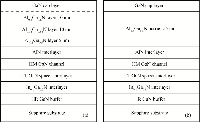
Fig. 1.
Schematics of investigated HEMT structures. (a) The step-graded structure. (b) The high Al structure.
SEMICONDUCTOR MATERIALS
Jian Tang1, , Xiaoliang Wang2 and Hongling Xiao2
Corresponding author: Tang Jian, Email:jtang@semi.ac.cn
Abstract: A novel InGaN back barrier high electron mobility transistors structure with a compositionally step-graded AlGaN barrier layer was grown by metal organic chemical vapor deposition on sapphire substrate. The structural and electrical properties of two samples were investigated and compared:the first sample is the step-graded structure and the second one is the high Al structure as a comparison. By calculating full width at half maximum of XRD measurements, the densities of screw-type threading dislocations are 8.34×108 cm-2 and 11.44×108 cm-2 for step-graded structure and high Al structure, respectively, which are consistent with the results of atomic force microscopy. By Hall measurements, the measured two-dimensional electron gas mobility was 1820 cm2/(V·s) for step-graded structure, and 1300 cm2/(V·s) for high Al structure, respectively. The step-graded structure improves the crystal quality of AlGaN layer due to the released lattice strain. The device was fabricated and leakage current is only 28 μA when the drain voltage is 10 V; it was found that the InGaN back barrier could effectively reduce the buffer leakage current.
Keywords: GaN, HEMT, back barrier, step-graded
| [1] |
Wang X L, Cheng T S, Xiao H L, et al. An internally-matched GaN HEMTs device with 45.2 W at 8 GHz for X-band application. Solid-State Electron, 2009, 53:332 doi: 10.1016/j.sse.2009.01.003
|
| [2] |
Ren Chunjiang, Li Zhonghui, Yu Xuming, et al. Field plated 0.15μm GaN HEMTs for millimeter-wave application. Journal of Semiconductors, 2013, 34(6):064002 doi: 10.1088/1674-4926/34/6/064002
|
| [3] |
Wang Jianhui, Wang Xinhua, Pan Lei, et al. Effect of varying layouts on the gate temperature for multi-finger AlGaN/GaN HEMTs. Journal of Semiconductors, 2012, 33(9):094004 doi: 10.1088/1674-4926/33/9/094004
|
| [4] |
Zhang Renping, Yan Wei, Wang Xiaoliang, et al. Fabrication and characterization of high performance AlGaN/GaN HEMTs on sapphire with silicon nitride passivation. Journal of Semiconductors, 2011, 32(6):064001 doi: 10.1088/1674-4926/32/6/064001
|
| [5] |
Manuel J M, Morales F M, Garcia R, et al. Threading dislocation propagation in AlGaN/GaN based HEMT structures grown on Si (111) by plasma assisted molecular beam epitaxy. J Cryst Growth, 2012, 357:35 doi: 10.1016/j.jcrysgro.2012.07.037
|
| [6] |
Schuette M L, Ketterson A, Song B, et al. Gate-recessed integrated E/D GaN HEMT technology with fT/fmax > 300 GHz. IEEE Electron Device Lett, 2013, 34(6):741 doi: 10.1109/LED.2013.2257657
|
| [7] |
Benyahya N, Mazari H, Benseddik N, et al. Characterization and comparison between Ig(Vgs) structures HEMT AlInN/GaN and AlGaN/GaN. Opt Quantum Electron, 2014, 46(1):209 doi: 10.1007/s11082-013-9747-4
|
| [8] |
Palacios T, Chakraborty A, Heikman S, et al. AlGaN/GaN high electron mobility transistors with InGaN back-barriers. IEEE Electron Device Lett, 2006, 27:13 doi: 10.1109/LED.2005.860882
|
| [9] |
Tang J, Wang X, Chen T, et al. AlGaN/AlN/GaN/InGaN/GaN DH-HEMTs with improved mobility grown by MOCVD. 9th International Conference on Solid-State and Integrated-Circuit Technology, ICSICT, 2008:1114 http://ieeexplore.ieee.org/xpls/abs_all.jsp?arnumber=4734732
|
| [10] |
Shi Linyu, Zhang Jincheng, Wang Hao, et al. Growth of InGaN and double heterojunction structure with InGaN back barrier. Journal of Semiconductors, 2010, 31(12):123001 doi: 10.1088/1674-4926/31/12/123001
|
| [11] |
Ma Z Y, Wang X L, Hu G X, et al. Growth and characterization of AlGaN/AlN/GaN HEMT structures with a compositionally step-graded AlGaN barrier layer. Chin Phys Lett, 2007, 24:1705 doi: 10.1088/0256-307X/24/6/075
|
| [12] |
Moram M A, Vickers M E. X-ray diffraction of Ⅲ-nitrides. Reports on Progress in Physics, 2009, 72:036502 doi: 10.1088/0034-4885/72/3/036502
|
| [13] |
Lu L, Shen B, Xu F J, et al. Morphology of threading dislocations in high-resistivity GaN films observed by transmission electron microscopy. J Appl Phys, 2007, 102(3):033510 doi: 10.1063/1.2768015
|
| [14] |
Srikant V, Speck J S, Clarke D R. Mosaic structure in epitaxial thin films having large lattice mismatch. J Appl Phys, 1997, 82(9):4286 doi: 10.1063/1.366235
|
| [15] |
Khoury M, Courville A, Poulet B, et al. Imaging and counting threading dislocations in c-oriented epitaxial GaN layers. Semicond Sci Technol, 2013, 28:035006 doi: 10.1088/0268-1242/28/3/035006
|
| [16] |
Shen L, Heikman S, Moran B, et al. AlGaN/AlN/GaN high-power microwave HEMT. IEEE Electron Device Lett, 2001, 22:457 doi: 10.1109/55.954910
|
| [17] |
Skierbiszewski C, Wasilewski Z, Siekacz M, et al. Growth optimisation of the GaN layers and GaN/AlGaN heterojunctions on bulk GaN substrates using plasma-assisted molecular beam epitaxy. Phys Status Solidi A, 2004, 201(2):320 doi: 10.1002/(ISSN)1521-396X
|
| [18] |
Ran J X, Wang X L, Hu G X, et al. Characteristics of InGaN channel HEMTs grown by MOCVD. 8th International Conference on Solid-State and Integrated Circuit Technology, 2006, 2:929 http://ieeexplore.ieee.org/xpls/abs_all.jsp?arnumber=4098280
|
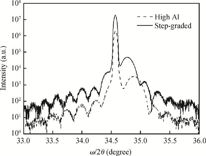

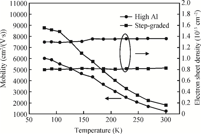
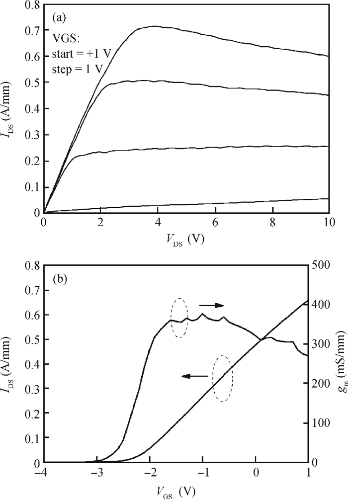
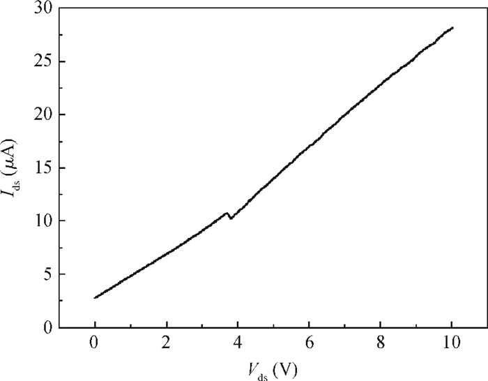
Table 1.
The electrical properties obtained by Hall measurements, (0002) FWHMs and calculated dislocation densities, as well as data from 2

|
Table 2.
Lattice mismatch

|
| [1] |
Wang X L, Cheng T S, Xiao H L, et al. An internally-matched GaN HEMTs device with 45.2 W at 8 GHz for X-band application. Solid-State Electron, 2009, 53:332 doi: 10.1016/j.sse.2009.01.003
|
| [2] |
Ren Chunjiang, Li Zhonghui, Yu Xuming, et al. Field plated 0.15μm GaN HEMTs for millimeter-wave application. Journal of Semiconductors, 2013, 34(6):064002 doi: 10.1088/1674-4926/34/6/064002
|
| [3] |
Wang Jianhui, Wang Xinhua, Pan Lei, et al. Effect of varying layouts on the gate temperature for multi-finger AlGaN/GaN HEMTs. Journal of Semiconductors, 2012, 33(9):094004 doi: 10.1088/1674-4926/33/9/094004
|
| [4] |
Zhang Renping, Yan Wei, Wang Xiaoliang, et al. Fabrication and characterization of high performance AlGaN/GaN HEMTs on sapphire with silicon nitride passivation. Journal of Semiconductors, 2011, 32(6):064001 doi: 10.1088/1674-4926/32/6/064001
|
| [5] |
Manuel J M, Morales F M, Garcia R, et al. Threading dislocation propagation in AlGaN/GaN based HEMT structures grown on Si (111) by plasma assisted molecular beam epitaxy. J Cryst Growth, 2012, 357:35 doi: 10.1016/j.jcrysgro.2012.07.037
|
| [6] |
Schuette M L, Ketterson A, Song B, et al. Gate-recessed integrated E/D GaN HEMT technology with fT/fmax > 300 GHz. IEEE Electron Device Lett, 2013, 34(6):741 doi: 10.1109/LED.2013.2257657
|
| [7] |
Benyahya N, Mazari H, Benseddik N, et al. Characterization and comparison between Ig(Vgs) structures HEMT AlInN/GaN and AlGaN/GaN. Opt Quantum Electron, 2014, 46(1):209 doi: 10.1007/s11082-013-9747-4
|
| [8] |
Palacios T, Chakraborty A, Heikman S, et al. AlGaN/GaN high electron mobility transistors with InGaN back-barriers. IEEE Electron Device Lett, 2006, 27:13 doi: 10.1109/LED.2005.860882
|
| [9] |
Tang J, Wang X, Chen T, et al. AlGaN/AlN/GaN/InGaN/GaN DH-HEMTs with improved mobility grown by MOCVD. 9th International Conference on Solid-State and Integrated-Circuit Technology, ICSICT, 2008:1114 http://ieeexplore.ieee.org/xpls/abs_all.jsp?arnumber=4734732
|
| [10] |
Shi Linyu, Zhang Jincheng, Wang Hao, et al. Growth of InGaN and double heterojunction structure with InGaN back barrier. Journal of Semiconductors, 2010, 31(12):123001 doi: 10.1088/1674-4926/31/12/123001
|
| [11] |
Ma Z Y, Wang X L, Hu G X, et al. Growth and characterization of AlGaN/AlN/GaN HEMT structures with a compositionally step-graded AlGaN barrier layer. Chin Phys Lett, 2007, 24:1705 doi: 10.1088/0256-307X/24/6/075
|
| [12] |
Moram M A, Vickers M E. X-ray diffraction of Ⅲ-nitrides. Reports on Progress in Physics, 2009, 72:036502 doi: 10.1088/0034-4885/72/3/036502
|
| [13] |
Lu L, Shen B, Xu F J, et al. Morphology of threading dislocations in high-resistivity GaN films observed by transmission electron microscopy. J Appl Phys, 2007, 102(3):033510 doi: 10.1063/1.2768015
|
| [14] |
Srikant V, Speck J S, Clarke D R. Mosaic structure in epitaxial thin films having large lattice mismatch. J Appl Phys, 1997, 82(9):4286 doi: 10.1063/1.366235
|
| [15] |
Khoury M, Courville A, Poulet B, et al. Imaging and counting threading dislocations in c-oriented epitaxial GaN layers. Semicond Sci Technol, 2013, 28:035006 doi: 10.1088/0268-1242/28/3/035006
|
| [16] |
Shen L, Heikman S, Moran B, et al. AlGaN/AlN/GaN high-power microwave HEMT. IEEE Electron Device Lett, 2001, 22:457 doi: 10.1109/55.954910
|
| [17] |
Skierbiszewski C, Wasilewski Z, Siekacz M, et al. Growth optimisation of the GaN layers and GaN/AlGaN heterojunctions on bulk GaN substrates using plasma-assisted molecular beam epitaxy. Phys Status Solidi A, 2004, 201(2):320 doi: 10.1002/(ISSN)1521-396X
|
| [18] |
Ran J X, Wang X L, Hu G X, et al. Characteristics of InGaN channel HEMTs grown by MOCVD. 8th International Conference on Solid-State and Integrated Circuit Technology, 2006, 2:929 http://ieeexplore.ieee.org/xpls/abs_all.jsp?arnumber=4098280
|


Article views: 3215 Times PDF downloads: 33 Times Cited by: 0 Times
Received: 05 March 2014 Revised: 05 May 2014 Online: Published: 01 November 2014
| Citation: |
Jian Tang, Xiaoliang Wang, Hongling Xiao. Growth and characterization of InGaN back barrier HEMTs structure with a compositionally step-graded AlGaN layer[J]. Journal of Semiconductors, 2014, 35(11): 113006. doi: 10.1088/1674-4926/35/11/113006
****
J Tang, X L Wang, H L Xiao. Growth and characterization of InGaN back barrier HEMTs structure with a compositionally step-graded AlGaN layer[J]. J. Semicond., 2014, 35(11): 113006. doi: 10.1088/1674-4926/35/11/113006.

|
| [1] |
Wang X L, Cheng T S, Xiao H L, et al. An internally-matched GaN HEMTs device with 45.2 W at 8 GHz for X-band application. Solid-State Electron, 2009, 53:332 doi: 10.1016/j.sse.2009.01.003
|
| [2] |
Ren Chunjiang, Li Zhonghui, Yu Xuming, et al. Field plated 0.15μm GaN HEMTs for millimeter-wave application. Journal of Semiconductors, 2013, 34(6):064002 doi: 10.1088/1674-4926/34/6/064002
|
| [3] |
Wang Jianhui, Wang Xinhua, Pan Lei, et al. Effect of varying layouts on the gate temperature for multi-finger AlGaN/GaN HEMTs. Journal of Semiconductors, 2012, 33(9):094004 doi: 10.1088/1674-4926/33/9/094004
|
| [4] |
Zhang Renping, Yan Wei, Wang Xiaoliang, et al. Fabrication and characterization of high performance AlGaN/GaN HEMTs on sapphire with silicon nitride passivation. Journal of Semiconductors, 2011, 32(6):064001 doi: 10.1088/1674-4926/32/6/064001
|
| [5] |
Manuel J M, Morales F M, Garcia R, et al. Threading dislocation propagation in AlGaN/GaN based HEMT structures grown on Si (111) by plasma assisted molecular beam epitaxy. J Cryst Growth, 2012, 357:35 doi: 10.1016/j.jcrysgro.2012.07.037
|
| [6] |
Schuette M L, Ketterson A, Song B, et al. Gate-recessed integrated E/D GaN HEMT technology with fT/fmax > 300 GHz. IEEE Electron Device Lett, 2013, 34(6):741 doi: 10.1109/LED.2013.2257657
|
| [7] |
Benyahya N, Mazari H, Benseddik N, et al. Characterization and comparison between Ig(Vgs) structures HEMT AlInN/GaN and AlGaN/GaN. Opt Quantum Electron, 2014, 46(1):209 doi: 10.1007/s11082-013-9747-4
|
| [8] |
Palacios T, Chakraborty A, Heikman S, et al. AlGaN/GaN high electron mobility transistors with InGaN back-barriers. IEEE Electron Device Lett, 2006, 27:13 doi: 10.1109/LED.2005.860882
|
| [9] |
Tang J, Wang X, Chen T, et al. AlGaN/AlN/GaN/InGaN/GaN DH-HEMTs with improved mobility grown by MOCVD. 9th International Conference on Solid-State and Integrated-Circuit Technology, ICSICT, 2008:1114 http://ieeexplore.ieee.org/xpls/abs_all.jsp?arnumber=4734732
|
| [10] |
Shi Linyu, Zhang Jincheng, Wang Hao, et al. Growth of InGaN and double heterojunction structure with InGaN back barrier. Journal of Semiconductors, 2010, 31(12):123001 doi: 10.1088/1674-4926/31/12/123001
|
| [11] |
Ma Z Y, Wang X L, Hu G X, et al. Growth and characterization of AlGaN/AlN/GaN HEMT structures with a compositionally step-graded AlGaN barrier layer. Chin Phys Lett, 2007, 24:1705 doi: 10.1088/0256-307X/24/6/075
|
| [12] |
Moram M A, Vickers M E. X-ray diffraction of Ⅲ-nitrides. Reports on Progress in Physics, 2009, 72:036502 doi: 10.1088/0034-4885/72/3/036502
|
| [13] |
Lu L, Shen B, Xu F J, et al. Morphology of threading dislocations in high-resistivity GaN films observed by transmission electron microscopy. J Appl Phys, 2007, 102(3):033510 doi: 10.1063/1.2768015
|
| [14] |
Srikant V, Speck J S, Clarke D R. Mosaic structure in epitaxial thin films having large lattice mismatch. J Appl Phys, 1997, 82(9):4286 doi: 10.1063/1.366235
|
| [15] |
Khoury M, Courville A, Poulet B, et al. Imaging and counting threading dislocations in c-oriented epitaxial GaN layers. Semicond Sci Technol, 2013, 28:035006 doi: 10.1088/0268-1242/28/3/035006
|
| [16] |
Shen L, Heikman S, Moran B, et al. AlGaN/AlN/GaN high-power microwave HEMT. IEEE Electron Device Lett, 2001, 22:457 doi: 10.1109/55.954910
|
| [17] |
Skierbiszewski C, Wasilewski Z, Siekacz M, et al. Growth optimisation of the GaN layers and GaN/AlGaN heterojunctions on bulk GaN substrates using plasma-assisted molecular beam epitaxy. Phys Status Solidi A, 2004, 201(2):320 doi: 10.1002/(ISSN)1521-396X
|
| [18] |
Ran J X, Wang X L, Hu G X, et al. Characteristics of InGaN channel HEMTs grown by MOCVD. 8th International Conference on Solid-State and Integrated Circuit Technology, 2006, 2:929 http://ieeexplore.ieee.org/xpls/abs_all.jsp?arnumber=4098280
|

 WeChat ID
Journal of Semiconductors © 2017 All Rights Reserved 京ICP备05085259号-2

 DownLoad:

