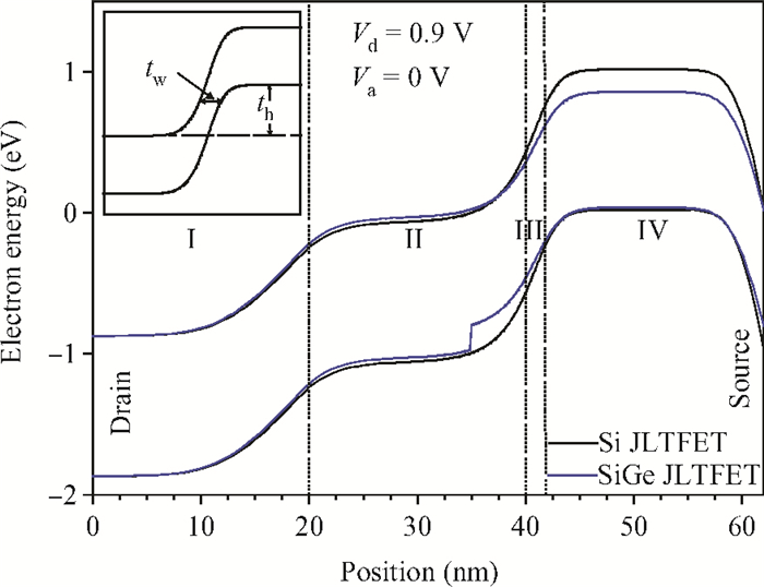
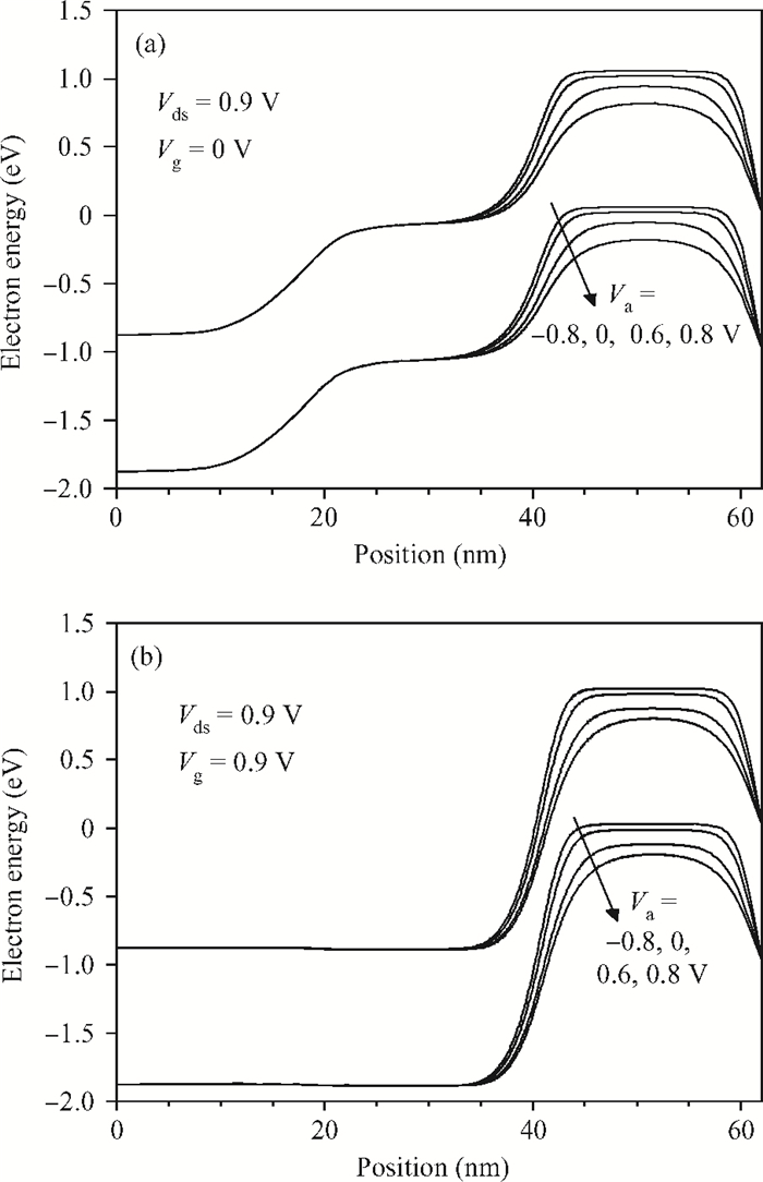
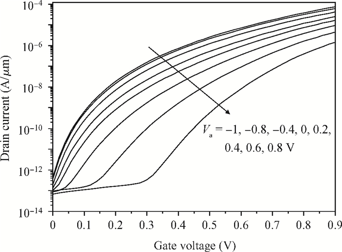
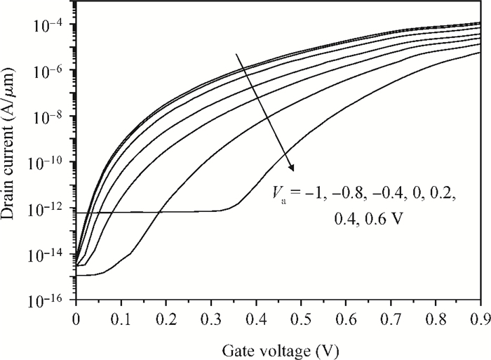
| [1] |
Riel H, Ionescu A M. Tunnel field-effect transistors as energy-efficient electronic switches. Nature, 2011, 479:329 doi: 10.1038/nature10679 |
| [2] |
Koswatta S O, Lundstrom M S, Nikonov D E. Performance comparison between p-i-n tunneling transistors and conventional MOSFETs. IEEE Trans Electron Devices, 2009, 56:456 doi: 10.1109/TED.2008.2011934 |
| [3] |
Boucart K, Ionescu A M. Double-gate tunnel fet with high-k gate dielectric. IEEE Trans Electron Devices, 2007, 54:1725 doi: 10.1109/TED.2007.899389 |
| [4] |
Boucart K, Ionescu A M. Length scaling of the double gate tunnel FET with a high-k gate dielectric. Solid-State Electron, 2007, 51:1500 doi: 10.1016/j.sse.2007.09.014 |
| [5] |
Kim S H, Agarwal S, Jacobson Z A, et al. Tunnel field effect transistor with raised germanium source. IEEE Electron Device Lett, 2010, 31:1107 doi: 10.1109/LED.2010.2061214 |
| [6] |
|
| [7] |
Patel N, Ramesha A, Mahapatra S. Drive current boosting of n-type tunnel FET with strained SiGe layer at source. Microelectron J, 2008, 39:1671 doi: 10.1016/j.mejo.2008.02.020 |
| [8] |
Toh E H, Wang G H, Chan L, et al. Device physics and guiding principles for the design of double-gate tunne ling field effect transistor with silicon-germanium source heterojunction. Appl Phys Lett, 2007, 91:243505 doi: 10.1063/1.2823606 |
| [9] |
Shih C, Chien N D. Sub-10-nm tunnel field-effect transistor with graded Si/Ge heterojunction. IEEE Electron Device Lett, 2011, 32:1498 doi: 10.1109/LED.2011.2164512 |
| [10] |
|
| [11] |
Moselund K E, Schmid H, Bessire C, et al. InAs-Si nanowire heterojunction tunnel FETs. IEEE Electron Device Lett, 2012, 33:1453 doi: 10.1109/LED.2012.2206789 |
| [12] |
Li R, Lu Y, Zhou G, et al. AlGaSb/InAs tunnel field-effect transistor with on-current of 78 μA/ μm at 0.5 V. IEEE Electron Device Lett, 2012, 33:363 doi: 10.1109/LED.2011.2179915 |
| [13] |
|
| [14] |
Bhuwalka K K, Sedlmaier S, Ludsteck A K, et al. Vertical tunnel field-effect transistor. IEEE Trans Electron Devices, 2004, 51:279 doi: 10.1109/TED.2003.821575 |
| [15] |
Chen J, Klaumnzer S, Lux-Steiner M C, et al. Vertical nanowire transistors with low leakage current. Appl Phys Lett, 2004, 85:1401 doi: 10.1063/1.1784037 |
| [16] |
Mookerjea S, Mohata D, Mayer T, et al. Temperature-dependent I- V characteristics of a vertical In 0.53Ga 0.47As tunnel FET. IEEE Electron Device Lett, 2010, 31:564 doi: 10.1109/LED.2010.2045631 |
| [17] |
Bhuwalka K K, Schulze J, Eisele I. Performance enhancement of vertical tunnel field-effect transistor with SiGe in the δp + layer. Jpn J Appl Phys, 2004, 43:4073 doi: 10.1143/JJAP.43.4073 |
| [18] |
Bhuwalka K K, Schulze J, Eisele I. Scaling the vertical tunnel FET with tunnel bandgap modulation and gate workfunction engineering. IEEE Trans Electron Devices, 2005, 52:909 doi: 10.1109/TED.2005.846318 |
| [19] |
Bal P, Akram M W, Mondal P, et al. Performance estimation of sub-30 nm junctionless tunnel FET (JLTFET). J Comput Electron, 2013, 12:782 doi: 10.1007/s10825-013-0483-6 |
| [20] |
Ghosh B, Akram M W. Junctionless tunnel field effect transistor. IEEE Electron Device Lett, 2013, 34:584 doi: 10.1109/LED.2013.2253752 |
| [21] |
Mondal P, Ghosh B, Bal P. Planar junctionless transistor with non-uniform channel doping. Appl Phys Lett, 2013, 102:133505 doi: 10.1063/1.4801443 |
| [22] |
Bal P, Ghosh B, Mondal P, et al. Dual material gate junctionless tunnel field effect transistor. J Comput Electron, 2014, 13:230 doi: 10.1007/s10825-013-0505-4 |
| [23] |
Assaderaghi F, Sinitsky D, Parke S A, et al. Dynamic threshold-voltage MOSFET (DTMOS) for ultra-low voltage VLSI. IEEE Trans Electron Devices, 1997, 44:414 doi: 10.1109/16.556151 |
| [24] |
|
| [25] |
|
| [26] |
SILVACO, ATLAS User's Manual, 2011
|
| [27] |
Schenk A. A model for the field and temperature dependence of Shockley-Read-Hall lifetimes in silicon. Solid-State Electron, 1992, 35:1585 doi: 10.1016/0038-1101(92)90184-E |
| [28] |
Crowell C R, Rideout V L. Normalized thermionic-field (T-F) emission in metal-semiconductor (Schottky) barriers. Solid-State Electron, 1969, 12:89 doi: 10.1016/0038-1101(69)90117-8 |
| [29] |
Murphy E L, Good R H. Thermionic emission, field emission, and the transition region. Phys Rev, 1956, 102:1464 doi: 10.1103/PhysRev.102.1464 |
| [30] |
Crowell C R, Sze S M. Current transport in metal-semiconductor barriers. Solid-State Electron, 1966, 9:1035 doi: 10.1016/0038-1101(66)90127-4 |
| [31] |
Mookerjea S, Krishnan R, Datta S, et al. Effective capacitance and drive current for tunnel FET (TFET) CV/I estimation. IEEE Trans Electron Devices, 2009, 56:2092 doi: 10.1109/TED.2009.2026516 |


 DownLoad: