


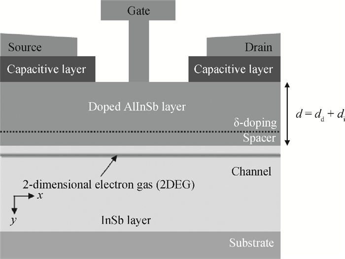
Fig. 1.
Cross sectional view of single gate AlInSb/InSb HEMT.
SEMICONDUCTOR DEVICES
S. Theodore Chandra, N.B. Balamurugan, G. Subalakshmi, T. Shalini and G. Lakshmi Priya
Corresponding author: S. Theodore Chandra, Email: theodore@tce.edu
Abstract: We have developed a 2D analytical model for the single gate AlInSb/InSb HEMT device by solving the Poisson equation using the parabolic approximation method. The developed model analyses the device performance by calculating the parameters such as surface potential, electric field distribution and drain current. The high mobility of the AlInSb/InSb quantum makes this HEMT ideal for high frequency, high power applications. The working of the single gate AlInSb/InSb HEMT device is studied by considering the variation of gate source voltage, drain source voltage, and channel length under the gate region and temperature. The carrier transport efficiency is improved by uniform electric field along the channel and the peak values near the source and drain regions. The results from the analytical model are compared with that of numerical simulations (TCAD) and a good agreement between them is achieved.
Keywords: high electron mobility transistor, AlInSb/InSb quantum well, 2D analytical model, Poisson's equation, surface potential, electric field
| [1] |
Ambacher O. Growth and applications of group Ⅲ-nitrides. J Phys D:Appl Phys, 1998, 31:2653 doi: 10.1088/0022-3727/31/20/001
|
| [2] |
Paskova T, Hanser D A, Evans K R. GaN substrate for Ⅲ nitride devices. IEEE Trans Electron Devices, 2010, 98(7):1324
|
| [3] |
Palacios T, Chakraborty A, Heikman S, et al. AlGaN/GaN high electron mobility transistors with InGaN back-barriers. IEEE Electron Device Lett, 2006, 27(1):13 doi: 10.1109/LED.2005.860882
|
| [4] |
Kruppa W, Boos J B, Bennett B R, et al. Low-frequency noise in AlSb/InAs and related HEMTs. IEEE Trans Electron Devices, 2007, 54(5):1193 doi: 10.1109/TED.2007.893658
|
| [5] |
Kharche1 N, Klimeck G, Kim D H, et al. Performance analysis of ultra-scaled InAs HEMTs. IEEE International Electron Devices Meeting (IEDM), 2009:1 http://ieeexplore.ieee.org/xpls/icp.jsp?arnumber=5424315
|
| [6] |
Moschetti G, Zhao H, Nilsson P A, et al. Anisotropic transport properties in InAs/AlSb heterostructures. Appl Phys Lett, 2010, 97:243510 doi: 10.1063/1.3527971
|
| [7] |
Ohno Y, Kuzuhara M. Application of GaN-based heterojunction FETs for advanced wireless communication. IEEE Trans Electron Devices, 2001, 48(3):517 doi: 10.1109/16.906445
|
| [8] |
Boos J B, Bennett B R, Papanicolaou N A, et al. Sb-based n-and p-channel heterostructure FETs for high-speed, low-power applications. IEICE Trans Electron, 2008, E91-C(7):1050 doi: 10.1093/ietele/e91-c.7.1050
|
| [9] |
Kumar S P, Agrawal A, Chaujar R, et al. Threshold voltage model for small geometry AlGaN/GaN HEMTs based on analytical solution of 3-D Poisson's equation. Microelectron J, 2007, 4, 38:1013 http://dl.acm.org/citation.cfm?id=1316173
|
| [10] |
Yoon S F, Gay B P, Zheng H Q, et al. Fabrication of strained and double heterojunction InGaP/InGaAs high electron mobility transistors grown by solid-source molecular beam epitaxy. IEEE Trans Electron Devices, 2000, 47(5):2255
|
| [11] |
Khandelwal S, Goyal N, Fjedly A T. A physics-based analytical model for 2DEG charge density in AlGaN/GaN HEMT devices. IEEE Trans Electron Devices, 2011, 58(10):3622 doi: 10.1109/TED.2011.2161314
|
| [12] |
Lee K, Shur M S, Drummond T J, et al. Current-voltage and capacitance-voltage characteristics of modulation-doped field-effect transistors. IEEE Trans Electron Devices, 1983, 30(3):207 doi: 10.1109/T-ED.1983.21101
|
| [13] |
Lin J C, Yang P Y, Tsai W C. Simulation and analysis of metamorphic high electron mobility transistors. Microelectron J, 2007, 38:251 doi: 10.1016/j.mejo.2006.11.004
|
| [14] |
Colinge J P. FinFETs and other multi-gate transistors. Springer, 2007 http://dl.acm.org/citation.cfm?id=1564890
|
| [15] |
Sentaurus Device User Guide, Synopsys Inc. , Version D-2010. 03
|
| [16] |
Sze S M. Physics of semiconductor devices. 2nd ed. New York:Wiley, 2004:438
|

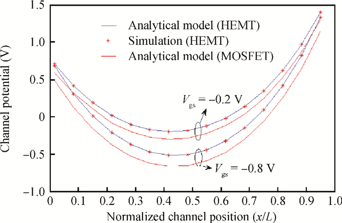
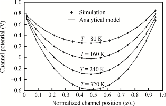
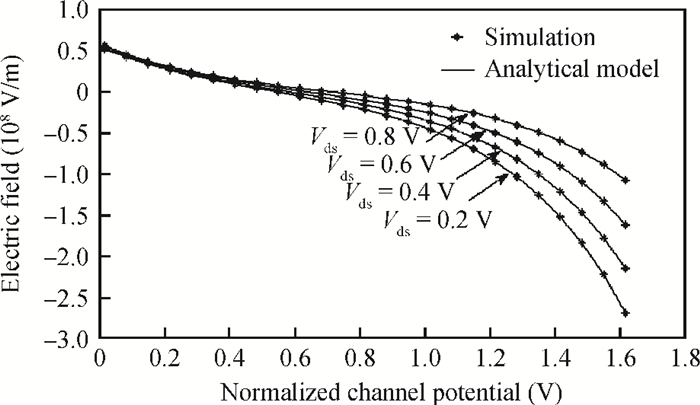
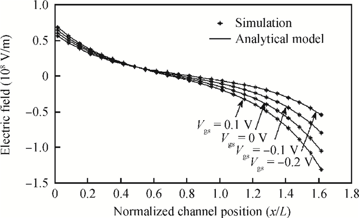
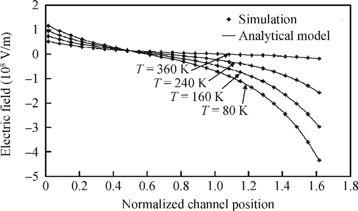
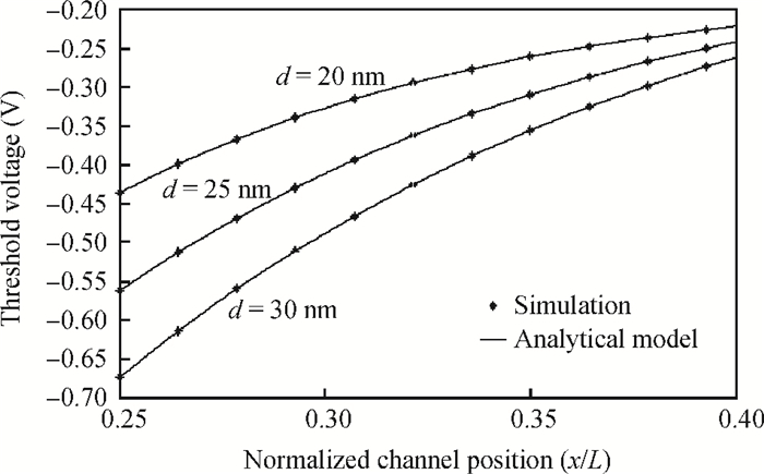
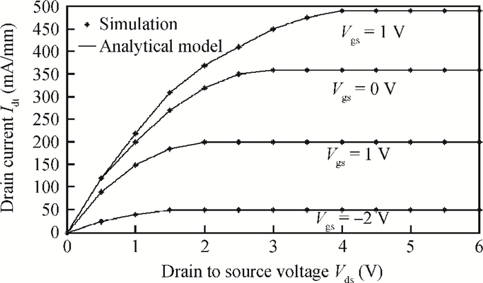
Table 1. Symbols and values.

|
| [1] |
Ambacher O. Growth and applications of group Ⅲ-nitrides. J Phys D:Appl Phys, 1998, 31:2653 doi: 10.1088/0022-3727/31/20/001
|
| [2] |
Paskova T, Hanser D A, Evans K R. GaN substrate for Ⅲ nitride devices. IEEE Trans Electron Devices, 2010, 98(7):1324
|
| [3] |
Palacios T, Chakraborty A, Heikman S, et al. AlGaN/GaN high electron mobility transistors with InGaN back-barriers. IEEE Electron Device Lett, 2006, 27(1):13 doi: 10.1109/LED.2005.860882
|
| [4] |
Kruppa W, Boos J B, Bennett B R, et al. Low-frequency noise in AlSb/InAs and related HEMTs. IEEE Trans Electron Devices, 2007, 54(5):1193 doi: 10.1109/TED.2007.893658
|
| [5] |
Kharche1 N, Klimeck G, Kim D H, et al. Performance analysis of ultra-scaled InAs HEMTs. IEEE International Electron Devices Meeting (IEDM), 2009:1 http://ieeexplore.ieee.org/xpls/icp.jsp?arnumber=5424315
|
| [6] |
Moschetti G, Zhao H, Nilsson P A, et al. Anisotropic transport properties in InAs/AlSb heterostructures. Appl Phys Lett, 2010, 97:243510 doi: 10.1063/1.3527971
|
| [7] |
Ohno Y, Kuzuhara M. Application of GaN-based heterojunction FETs for advanced wireless communication. IEEE Trans Electron Devices, 2001, 48(3):517 doi: 10.1109/16.906445
|
| [8] |
Boos J B, Bennett B R, Papanicolaou N A, et al. Sb-based n-and p-channel heterostructure FETs for high-speed, low-power applications. IEICE Trans Electron, 2008, E91-C(7):1050 doi: 10.1093/ietele/e91-c.7.1050
|
| [9] |
Kumar S P, Agrawal A, Chaujar R, et al. Threshold voltage model for small geometry AlGaN/GaN HEMTs based on analytical solution of 3-D Poisson's equation. Microelectron J, 2007, 4, 38:1013 http://dl.acm.org/citation.cfm?id=1316173
|
| [10] |
Yoon S F, Gay B P, Zheng H Q, et al. Fabrication of strained and double heterojunction InGaP/InGaAs high electron mobility transistors grown by solid-source molecular beam epitaxy. IEEE Trans Electron Devices, 2000, 47(5):2255
|
| [11] |
Khandelwal S, Goyal N, Fjedly A T. A physics-based analytical model for 2DEG charge density in AlGaN/GaN HEMT devices. IEEE Trans Electron Devices, 2011, 58(10):3622 doi: 10.1109/TED.2011.2161314
|
| [12] |
Lee K, Shur M S, Drummond T J, et al. Current-voltage and capacitance-voltage characteristics of modulation-doped field-effect transistors. IEEE Trans Electron Devices, 1983, 30(3):207 doi: 10.1109/T-ED.1983.21101
|
| [13] |
Lin J C, Yang P Y, Tsai W C. Simulation and analysis of metamorphic high electron mobility transistors. Microelectron J, 2007, 38:251 doi: 10.1016/j.mejo.2006.11.004
|
| [14] |
Colinge J P. FinFETs and other multi-gate transistors. Springer, 2007 http://dl.acm.org/citation.cfm?id=1564890
|
| [15] |
Sentaurus Device User Guide, Synopsys Inc. , Version D-2010. 03
|
| [16] |
Sze S M. Physics of semiconductor devices. 2nd ed. New York:Wiley, 2004:438
|


Article views: 3380 Times PDF downloads: 25 Times Cited by: 0 Times
Received: 30 April 2014 Revised: 09 June 2014 Online: Published: 01 November 2014
| Citation: |
S. Theodore Chandra, N.B. Balamurugan, G. Subalakshmi, T. Shalini, G. Lakshmi Priya. Compact analytical model for single gate AlInSb/InSb high electron mobility transistors[J]. Journal of Semiconductors, 2014, 35(11): 114003. doi: 10.1088/1674-4926/35/11/114003
****
S. T Chandra, N.B. Balamurugan, G. Subalakshmi, T. Shalini, G. L. Priya. Compact analytical model for single gate AlInSb/InSb high electron mobility transistors[J]. J. Semicond., 2014, 35(11): 114003. doi: 10.1088/1674-4926/35/11/114003.

|
| [1] |
Ambacher O. Growth and applications of group Ⅲ-nitrides. J Phys D:Appl Phys, 1998, 31:2653 doi: 10.1088/0022-3727/31/20/001
|
| [2] |
Paskova T, Hanser D A, Evans K R. GaN substrate for Ⅲ nitride devices. IEEE Trans Electron Devices, 2010, 98(7):1324
|
| [3] |
Palacios T, Chakraborty A, Heikman S, et al. AlGaN/GaN high electron mobility transistors with InGaN back-barriers. IEEE Electron Device Lett, 2006, 27(1):13 doi: 10.1109/LED.2005.860882
|
| [4] |
Kruppa W, Boos J B, Bennett B R, et al. Low-frequency noise in AlSb/InAs and related HEMTs. IEEE Trans Electron Devices, 2007, 54(5):1193 doi: 10.1109/TED.2007.893658
|
| [5] |
Kharche1 N, Klimeck G, Kim D H, et al. Performance analysis of ultra-scaled InAs HEMTs. IEEE International Electron Devices Meeting (IEDM), 2009:1 http://ieeexplore.ieee.org/xpls/icp.jsp?arnumber=5424315
|
| [6] |
Moschetti G, Zhao H, Nilsson P A, et al. Anisotropic transport properties in InAs/AlSb heterostructures. Appl Phys Lett, 2010, 97:243510 doi: 10.1063/1.3527971
|
| [7] |
Ohno Y, Kuzuhara M. Application of GaN-based heterojunction FETs for advanced wireless communication. IEEE Trans Electron Devices, 2001, 48(3):517 doi: 10.1109/16.906445
|
| [8] |
Boos J B, Bennett B R, Papanicolaou N A, et al. Sb-based n-and p-channel heterostructure FETs for high-speed, low-power applications. IEICE Trans Electron, 2008, E91-C(7):1050 doi: 10.1093/ietele/e91-c.7.1050
|
| [9] |
Kumar S P, Agrawal A, Chaujar R, et al. Threshold voltage model for small geometry AlGaN/GaN HEMTs based on analytical solution of 3-D Poisson's equation. Microelectron J, 2007, 4, 38:1013 http://dl.acm.org/citation.cfm?id=1316173
|
| [10] |
Yoon S F, Gay B P, Zheng H Q, et al. Fabrication of strained and double heterojunction InGaP/InGaAs high electron mobility transistors grown by solid-source molecular beam epitaxy. IEEE Trans Electron Devices, 2000, 47(5):2255
|
| [11] |
Khandelwal S, Goyal N, Fjedly A T. A physics-based analytical model for 2DEG charge density in AlGaN/GaN HEMT devices. IEEE Trans Electron Devices, 2011, 58(10):3622 doi: 10.1109/TED.2011.2161314
|
| [12] |
Lee K, Shur M S, Drummond T J, et al. Current-voltage and capacitance-voltage characteristics of modulation-doped field-effect transistors. IEEE Trans Electron Devices, 1983, 30(3):207 doi: 10.1109/T-ED.1983.21101
|
| [13] |
Lin J C, Yang P Y, Tsai W C. Simulation and analysis of metamorphic high electron mobility transistors. Microelectron J, 2007, 38:251 doi: 10.1016/j.mejo.2006.11.004
|
| [14] |
Colinge J P. FinFETs and other multi-gate transistors. Springer, 2007 http://dl.acm.org/citation.cfm?id=1564890
|
| [15] |
Sentaurus Device User Guide, Synopsys Inc. , Version D-2010. 03
|
| [16] |
Sze S M. Physics of semiconductor devices. 2nd ed. New York:Wiley, 2004:438
|

 WeChat ID
Journal of Semiconductors © 2017 All Rights Reserved 京ICP备05085259号-2

 DownLoad:

