


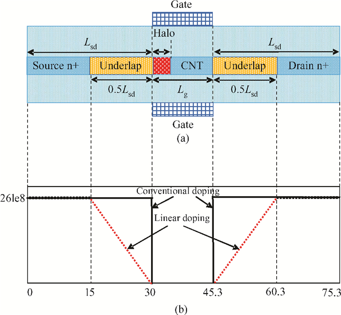
Fig. 1.
Cross-sectional view of the proposed CNTFET, it is symmetrical with respect to the center of the channel. The gate includes two metals with different work functions.
SEMICONDUCTOR DEVICES
Wei Wang1, , Lu Zhang1, Xueying Wang2, Zhubing Wang2, Ting Zhang1, Na Li1, Xiao Yang1 and Gongshu Yue1
Corresponding author: Wang Wei, Email:wangwej@njupt.edu.cn
Abstract: To overcome short-channel effects (SCEs) in high-performance device applications, a novel structure of CNTFET with a combination of halo and linear doping structure (HL-CNTFET) has been proposed. It has been theoretically investigated by a quantum kinetic model, which is based on two-dimensional non-equilibrium Green's functions solved self-consistently with Poisson's equations. We have studied the effect of halo doping and linear doping structure on static and dynamical performances of HL-CNTFET. It is demonstrated that a halo doping structure can decrease the drain leakage current and improve the on/off current ratio, and that linear doping can improve high-frequency and switching performance.
Keywords: CNTFET, NEGF, Halo doping, SCE, linear doping
| [1] |
Lu R F, Lu Y P, Lee S Y, et al. Terahertz response in single-walled carbon nanotube transistor:a real-time quantum dynamics simulation. Nanotechnology, 2009, 20(50):505401 doi: 10.1088/0957-4484/20/50/505401
|
| [2] |
Kienle D, Léonard F. Terahertz response of carbon nanotube transistors. Phys Rev Lett, 2000, 103(2):026601 http://www.tp1.physik.uni-bayreuth.de/de/publications/2009/Terahertz_Response_of_Carbon_Nanotube_Transistors/Terahertz_Response_of_Carbon_Nanotube_Transistors_Kienle__2009.pdf
|
| [3] |
Tans S J, Verschueren A R M, Dekker C. Room-temperature transistor based on a single carbon nanotube. Nature, 1998, 393(7):49 https://www.nature.com/nature/journal/v393/n6680/pdf/393049a0.pdf?foxtrotcallback=true
|
| [4] |
Shulaker M, Hills G, Patil N, et al. Carbon nanotube computer. Nature, 2013, 501(9):526 http://www.nature.com/nature/journal/v501/n7468/full/nature12502.html
|
| [5] |
Shulaker M, Rethy J V, Hills G, et al. Experimental demonstration of a fully digital capacitive sensor interface build entirely using carbon nanotube FETs. Proc Int Solid State Circuits Conf, 2013:112 http://ieeexplore.ieee.org/document/6487660/
|
| [6] |
Hazeghi A, Krishnamohan T, Wong H. Schottky-barrier carbon nanotube field-effect transistor modeling. IEEE Trans Electron Devices, 2007, 54(3):439 doi: 10.1109/TED.2006.890384
|
| [7] |
Guo J, Lundstrom M, Datta S. Performance projections for ballistic carbon nanotube field-effect transistors. Appl Phys Lett, 2002, 80(17):3192 doi: 10.1063/1.1474604
|
| [8] |
Fiori G, Iannaccone G, Klimeck G. A three-dimensional simulation study of the performance of carbon nanotube field-effect transistors with doped reservoirs and realistic geometry. IEEE Trans Electron Devices, 2006, 53(8):1782 doi: 10.1109/TED.2006.878018
|
| [9] |
Orouji A A, Arefinia Z. Detailed simulation study of a dual material gate carbon nanotube field-effect transistor. Phys E:Low-Dimensional Syst Nanostructures, 2009, 41(10):552 http://www.sciencedirect.com/science/article/pii/S1386947708003767
|
| [10] |
Liu X H, Zhao H L, Li T Y, et al. Improvement on the electron transport efficiency of the carbon nanotube field effect transistor device by introducing heterogeneous-dual-metal-gate structure. Acta Phys Sin, 2013, 62(14):147308 http://en.cnki.com.cn/Article_en/CJFDTotal-WLXB201314064.htm
|
| [11] |
Arefinia Z, Orouji A A. Quantum simulation study of a new carbon nanotube field-effect transistor with electrically induced source/drain extension. IEEE Trans Device Mater Reliab, 2009, 9(2):237 doi: 10.1109/TDMR.2009.2015458
|
| [12] |
Xia T S, Register L F, Banerjee S K. Simulation study of the carbon nanotube field effect transistors beyond the complex band structure effect. Solid-State Electron, 2005, 49(3):860 http://www.sciencedirect.com/science/article/pii/S003811010500064X
|
| [13] |
Guo J, Hasan S, Javey A, et al, Assessment of high-frequency performance potential for carbon nanotube transistors. IEEE Trans Nanotechnol, 2005, 4(6):715 doi: 10.1109/TNANO.2005.858601
|
| [14] |
Chen L, Pulfrey D L. Comparison of p-i-n and n-i-n carbon nanotube FETs regarding high-frequency performance. Solid-State Electron, 2009, 53(9):935 doi: 10.1016/j.sse.2009.05.006
|
| [15] |
Djeffal F, Meguellati M, Benhaya A. A two-dimensional analytical analysis of subthreshold behavior to study the scaling capability of nanoscale graded channel gate stack DG MOSFETs. Physica E:Low-Dimensional Systems and Nanostructures, 2009, 41(10):1872 doi: 10.1016/j.physe.2009.08.002
|
| [16] |
Reddy G V, Kumar M J. A new dual-material double-gate (DMDG) nanoscale SOI MOSFET-two-dimensional analytical modeling and simulation. IEEE Trans Nanotechnol, 2005, 4(2):260 doi: 10.1109/TNANO.2004.837845
|
| [17] |
Alam K, Lake R. Role of doping in carbon nanotube transistors with source/drain underlaps. IEEE Trans Nanotechnol, 2007, 6(6):652 doi: 10.1109/TNANO.2007.908170
|
| [18] |
Kordrostami Z, Sheikhi M H, Zarifkar A. Influence of channel and underlap engineering on the high-frequency and switching performance of CNTFETs. IEEE Trans Nanotechnol, 2012, 11(3):526 doi: 10.1109/TNANO.2011.2181998
|
| [19] |
Sarvari H, Ghayour R. Design of GNRFET using different doping profiles near the source and drain contacts. International Journal of Electronics, 2012, 99(5):673 doi: 10.1080/00207217.2011.643496
|
| [20] |
Zhang Z, Song S C, Huffman C. Integration of dual metal gate CMOS on high-k dielectrics utilizing a metal wet etch process. Electrochem Solid-State Lett, 2005, 8(10):G271 doi: 10.1149/1.2030447
|
| [21] |
Zhou C, Kong J, Yenilmez E, et al. Modulated chemical doping of individual carbon nanotubes. Science, 2000, 290(5496):1552 doi: 10.1126/science.290.5496.1552
|
| [22] |
Datta S. Nanoscale device modeling:the Green's function method. Superlatt Microstruct, 2000, 28(4):253 doi: 10.1006/spmi.2000.0920
|
| [23] |
Wang W, Li N, Ren Y, et al. A computational study of the effects of linear doping profile on the high-frequency and switching performances of hetero-material-gate CNTFETs. Journal of Semiconductors, 2013, 34(12):124002 doi: 10.1088/1674-4926/34/12/124002
|
| [24] |
Venugopal R, Ren Z, Datta S, et al. Simulating quantum transport in nanoscale CNTFETs:real versus mode-space approaches. J Appl Phys, 2002, 92(7):3730 doi: 10.1063/1.1503165
|
| [25] |
Wang W, Yang X, Li N, et al. Numerical study on the performance metrics of lightly doped drain and source grapheme nanoribbon field effect transistors with double-material-gate. Superlattices and Microstructures, 2013, 64(9):227 http://www.sciencedirect.com/science/article/pii/S0749603613003157
|
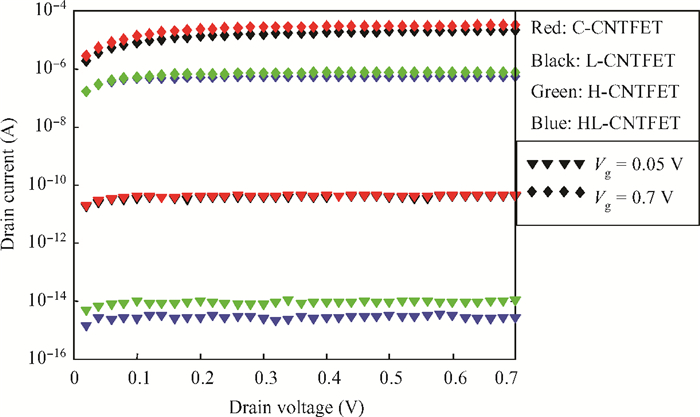
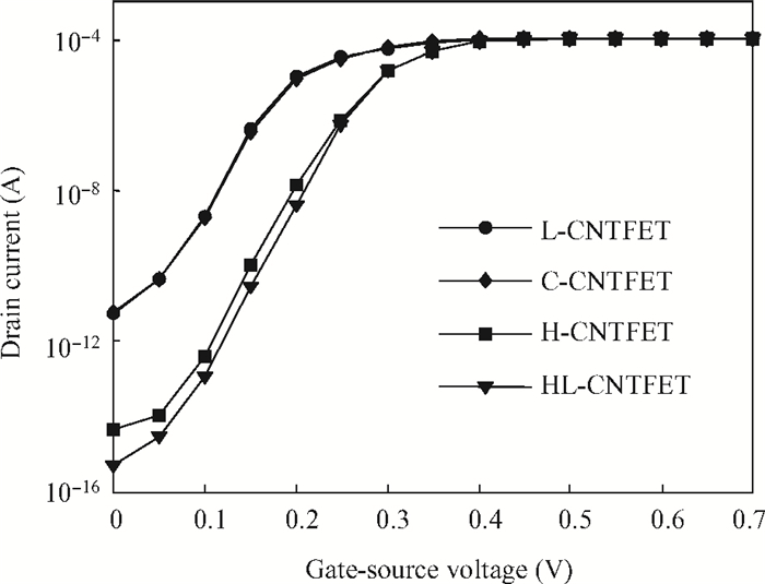
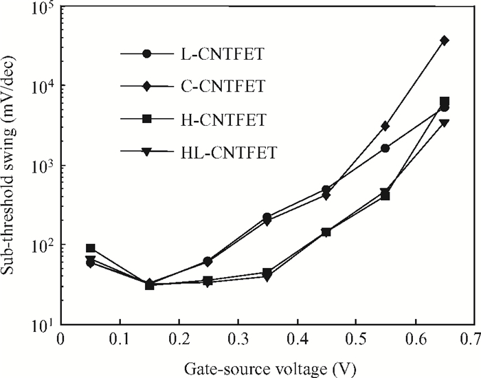


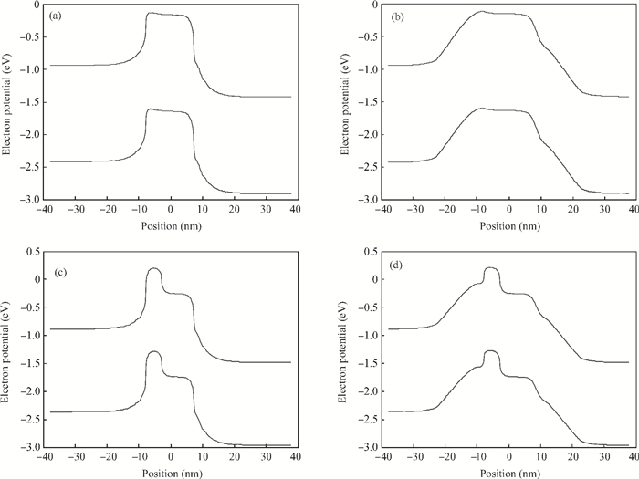
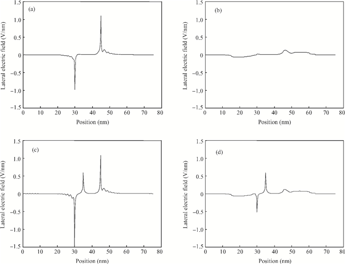
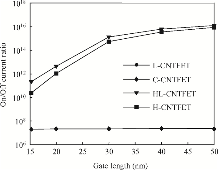
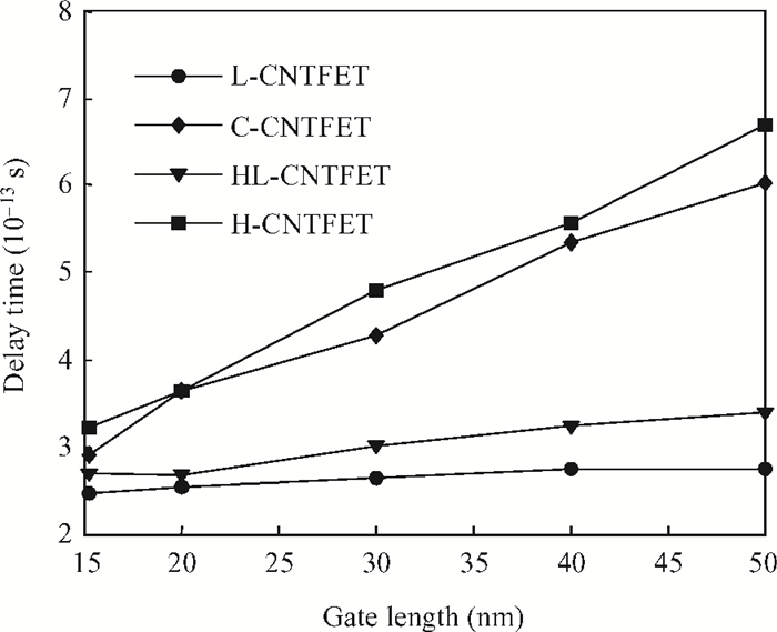

Table 1.
The

|
| [1] |
Lu R F, Lu Y P, Lee S Y, et al. Terahertz response in single-walled carbon nanotube transistor:a real-time quantum dynamics simulation. Nanotechnology, 2009, 20(50):505401 doi: 10.1088/0957-4484/20/50/505401
|
| [2] |
Kienle D, Léonard F. Terahertz response of carbon nanotube transistors. Phys Rev Lett, 2000, 103(2):026601 http://www.tp1.physik.uni-bayreuth.de/de/publications/2009/Terahertz_Response_of_Carbon_Nanotube_Transistors/Terahertz_Response_of_Carbon_Nanotube_Transistors_Kienle__2009.pdf
|
| [3] |
Tans S J, Verschueren A R M, Dekker C. Room-temperature transistor based on a single carbon nanotube. Nature, 1998, 393(7):49 https://www.nature.com/nature/journal/v393/n6680/pdf/393049a0.pdf?foxtrotcallback=true
|
| [4] |
Shulaker M, Hills G, Patil N, et al. Carbon nanotube computer. Nature, 2013, 501(9):526 http://www.nature.com/nature/journal/v501/n7468/full/nature12502.html
|
| [5] |
Shulaker M, Rethy J V, Hills G, et al. Experimental demonstration of a fully digital capacitive sensor interface build entirely using carbon nanotube FETs. Proc Int Solid State Circuits Conf, 2013:112 http://ieeexplore.ieee.org/document/6487660/
|
| [6] |
Hazeghi A, Krishnamohan T, Wong H. Schottky-barrier carbon nanotube field-effect transistor modeling. IEEE Trans Electron Devices, 2007, 54(3):439 doi: 10.1109/TED.2006.890384
|
| [7] |
Guo J, Lundstrom M, Datta S. Performance projections for ballistic carbon nanotube field-effect transistors. Appl Phys Lett, 2002, 80(17):3192 doi: 10.1063/1.1474604
|
| [8] |
Fiori G, Iannaccone G, Klimeck G. A three-dimensional simulation study of the performance of carbon nanotube field-effect transistors with doped reservoirs and realistic geometry. IEEE Trans Electron Devices, 2006, 53(8):1782 doi: 10.1109/TED.2006.878018
|
| [9] |
Orouji A A, Arefinia Z. Detailed simulation study of a dual material gate carbon nanotube field-effect transistor. Phys E:Low-Dimensional Syst Nanostructures, 2009, 41(10):552 http://www.sciencedirect.com/science/article/pii/S1386947708003767
|
| [10] |
Liu X H, Zhao H L, Li T Y, et al. Improvement on the electron transport efficiency of the carbon nanotube field effect transistor device by introducing heterogeneous-dual-metal-gate structure. Acta Phys Sin, 2013, 62(14):147308 http://en.cnki.com.cn/Article_en/CJFDTotal-WLXB201314064.htm
|
| [11] |
Arefinia Z, Orouji A A. Quantum simulation study of a new carbon nanotube field-effect transistor with electrically induced source/drain extension. IEEE Trans Device Mater Reliab, 2009, 9(2):237 doi: 10.1109/TDMR.2009.2015458
|
| [12] |
Xia T S, Register L F, Banerjee S K. Simulation study of the carbon nanotube field effect transistors beyond the complex band structure effect. Solid-State Electron, 2005, 49(3):860 http://www.sciencedirect.com/science/article/pii/S003811010500064X
|
| [13] |
Guo J, Hasan S, Javey A, et al, Assessment of high-frequency performance potential for carbon nanotube transistors. IEEE Trans Nanotechnol, 2005, 4(6):715 doi: 10.1109/TNANO.2005.858601
|
| [14] |
Chen L, Pulfrey D L. Comparison of p-i-n and n-i-n carbon nanotube FETs regarding high-frequency performance. Solid-State Electron, 2009, 53(9):935 doi: 10.1016/j.sse.2009.05.006
|
| [15] |
Djeffal F, Meguellati M, Benhaya A. A two-dimensional analytical analysis of subthreshold behavior to study the scaling capability of nanoscale graded channel gate stack DG MOSFETs. Physica E:Low-Dimensional Systems and Nanostructures, 2009, 41(10):1872 doi: 10.1016/j.physe.2009.08.002
|
| [16] |
Reddy G V, Kumar M J. A new dual-material double-gate (DMDG) nanoscale SOI MOSFET-two-dimensional analytical modeling and simulation. IEEE Trans Nanotechnol, 2005, 4(2):260 doi: 10.1109/TNANO.2004.837845
|
| [17] |
Alam K, Lake R. Role of doping in carbon nanotube transistors with source/drain underlaps. IEEE Trans Nanotechnol, 2007, 6(6):652 doi: 10.1109/TNANO.2007.908170
|
| [18] |
Kordrostami Z, Sheikhi M H, Zarifkar A. Influence of channel and underlap engineering on the high-frequency and switching performance of CNTFETs. IEEE Trans Nanotechnol, 2012, 11(3):526 doi: 10.1109/TNANO.2011.2181998
|
| [19] |
Sarvari H, Ghayour R. Design of GNRFET using different doping profiles near the source and drain contacts. International Journal of Electronics, 2012, 99(5):673 doi: 10.1080/00207217.2011.643496
|
| [20] |
Zhang Z, Song S C, Huffman C. Integration of dual metal gate CMOS on high-k dielectrics utilizing a metal wet etch process. Electrochem Solid-State Lett, 2005, 8(10):G271 doi: 10.1149/1.2030447
|
| [21] |
Zhou C, Kong J, Yenilmez E, et al. Modulated chemical doping of individual carbon nanotubes. Science, 2000, 290(5496):1552 doi: 10.1126/science.290.5496.1552
|
| [22] |
Datta S. Nanoscale device modeling:the Green's function method. Superlatt Microstruct, 2000, 28(4):253 doi: 10.1006/spmi.2000.0920
|
| [23] |
Wang W, Li N, Ren Y, et al. A computational study of the effects of linear doping profile on the high-frequency and switching performances of hetero-material-gate CNTFETs. Journal of Semiconductors, 2013, 34(12):124002 doi: 10.1088/1674-4926/34/12/124002
|
| [24] |
Venugopal R, Ren Z, Datta S, et al. Simulating quantum transport in nanoscale CNTFETs:real versus mode-space approaches. J Appl Phys, 2002, 92(7):3730 doi: 10.1063/1.1503165
|
| [25] |
Wang W, Yang X, Li N, et al. Numerical study on the performance metrics of lightly doped drain and source grapheme nanoribbon field effect transistors with double-material-gate. Superlattices and Microstructures, 2013, 64(9):227 http://www.sciencedirect.com/science/article/pii/S0749603613003157
|


Article views: 3750 Times PDF downloads: 21 Times Cited by: 0 Times
Received: 03 April 2014 Revised: 05 June 2014 Online: Published: 01 November 2014
| Citation: |
Wei Wang, Lu Zhang, Xueying Wang, Zhubing Wang, Ting Zhang, Na Li, Xiao Yang, Gongshu Yue. The combined effects of halo and linear doping effects on the high-frequency and switching performance in ballistic CNTFETs[J]. Journal of Semiconductors, 2014, 35(11): 114004. doi: 10.1088/1674-4926/35/11/114004
****
W Wang, L Zhang, X Y Wang, Z B Wang, T Zhang, N Li, X Yang, G S Yue. The combined effects of halo and linear doping effects on the high-frequency and switching performance in ballistic CNTFETs[J]. J. Semicond., 2014, 35(11): 114004. doi: 10.1088/1674-4926/35/11/114004.

|
| [1] |
Lu R F, Lu Y P, Lee S Y, et al. Terahertz response in single-walled carbon nanotube transistor:a real-time quantum dynamics simulation. Nanotechnology, 2009, 20(50):505401 doi: 10.1088/0957-4484/20/50/505401
|
| [2] |
Kienle D, Léonard F. Terahertz response of carbon nanotube transistors. Phys Rev Lett, 2000, 103(2):026601 http://www.tp1.physik.uni-bayreuth.de/de/publications/2009/Terahertz_Response_of_Carbon_Nanotube_Transistors/Terahertz_Response_of_Carbon_Nanotube_Transistors_Kienle__2009.pdf
|
| [3] |
Tans S J, Verschueren A R M, Dekker C. Room-temperature transistor based on a single carbon nanotube. Nature, 1998, 393(7):49 https://www.nature.com/nature/journal/v393/n6680/pdf/393049a0.pdf?foxtrotcallback=true
|
| [4] |
Shulaker M, Hills G, Patil N, et al. Carbon nanotube computer. Nature, 2013, 501(9):526 http://www.nature.com/nature/journal/v501/n7468/full/nature12502.html
|
| [5] |
Shulaker M, Rethy J V, Hills G, et al. Experimental demonstration of a fully digital capacitive sensor interface build entirely using carbon nanotube FETs. Proc Int Solid State Circuits Conf, 2013:112 http://ieeexplore.ieee.org/document/6487660/
|
| [6] |
Hazeghi A, Krishnamohan T, Wong H. Schottky-barrier carbon nanotube field-effect transistor modeling. IEEE Trans Electron Devices, 2007, 54(3):439 doi: 10.1109/TED.2006.890384
|
| [7] |
Guo J, Lundstrom M, Datta S. Performance projections for ballistic carbon nanotube field-effect transistors. Appl Phys Lett, 2002, 80(17):3192 doi: 10.1063/1.1474604
|
| [8] |
Fiori G, Iannaccone G, Klimeck G. A three-dimensional simulation study of the performance of carbon nanotube field-effect transistors with doped reservoirs and realistic geometry. IEEE Trans Electron Devices, 2006, 53(8):1782 doi: 10.1109/TED.2006.878018
|
| [9] |
Orouji A A, Arefinia Z. Detailed simulation study of a dual material gate carbon nanotube field-effect transistor. Phys E:Low-Dimensional Syst Nanostructures, 2009, 41(10):552 http://www.sciencedirect.com/science/article/pii/S1386947708003767
|
| [10] |
Liu X H, Zhao H L, Li T Y, et al. Improvement on the electron transport efficiency of the carbon nanotube field effect transistor device by introducing heterogeneous-dual-metal-gate structure. Acta Phys Sin, 2013, 62(14):147308 http://en.cnki.com.cn/Article_en/CJFDTotal-WLXB201314064.htm
|
| [11] |
Arefinia Z, Orouji A A. Quantum simulation study of a new carbon nanotube field-effect transistor with electrically induced source/drain extension. IEEE Trans Device Mater Reliab, 2009, 9(2):237 doi: 10.1109/TDMR.2009.2015458
|
| [12] |
Xia T S, Register L F, Banerjee S K. Simulation study of the carbon nanotube field effect transistors beyond the complex band structure effect. Solid-State Electron, 2005, 49(3):860 http://www.sciencedirect.com/science/article/pii/S003811010500064X
|
| [13] |
Guo J, Hasan S, Javey A, et al, Assessment of high-frequency performance potential for carbon nanotube transistors. IEEE Trans Nanotechnol, 2005, 4(6):715 doi: 10.1109/TNANO.2005.858601
|
| [14] |
Chen L, Pulfrey D L. Comparison of p-i-n and n-i-n carbon nanotube FETs regarding high-frequency performance. Solid-State Electron, 2009, 53(9):935 doi: 10.1016/j.sse.2009.05.006
|
| [15] |
Djeffal F, Meguellati M, Benhaya A. A two-dimensional analytical analysis of subthreshold behavior to study the scaling capability of nanoscale graded channel gate stack DG MOSFETs. Physica E:Low-Dimensional Systems and Nanostructures, 2009, 41(10):1872 doi: 10.1016/j.physe.2009.08.002
|
| [16] |
Reddy G V, Kumar M J. A new dual-material double-gate (DMDG) nanoscale SOI MOSFET-two-dimensional analytical modeling and simulation. IEEE Trans Nanotechnol, 2005, 4(2):260 doi: 10.1109/TNANO.2004.837845
|
| [17] |
Alam K, Lake R. Role of doping in carbon nanotube transistors with source/drain underlaps. IEEE Trans Nanotechnol, 2007, 6(6):652 doi: 10.1109/TNANO.2007.908170
|
| [18] |
Kordrostami Z, Sheikhi M H, Zarifkar A. Influence of channel and underlap engineering on the high-frequency and switching performance of CNTFETs. IEEE Trans Nanotechnol, 2012, 11(3):526 doi: 10.1109/TNANO.2011.2181998
|
| [19] |
Sarvari H, Ghayour R. Design of GNRFET using different doping profiles near the source and drain contacts. International Journal of Electronics, 2012, 99(5):673 doi: 10.1080/00207217.2011.643496
|
| [20] |
Zhang Z, Song S C, Huffman C. Integration of dual metal gate CMOS on high-k dielectrics utilizing a metal wet etch process. Electrochem Solid-State Lett, 2005, 8(10):G271 doi: 10.1149/1.2030447
|
| [21] |
Zhou C, Kong J, Yenilmez E, et al. Modulated chemical doping of individual carbon nanotubes. Science, 2000, 290(5496):1552 doi: 10.1126/science.290.5496.1552
|
| [22] |
Datta S. Nanoscale device modeling:the Green's function method. Superlatt Microstruct, 2000, 28(4):253 doi: 10.1006/spmi.2000.0920
|
| [23] |
Wang W, Li N, Ren Y, et al. A computational study of the effects of linear doping profile on the high-frequency and switching performances of hetero-material-gate CNTFETs. Journal of Semiconductors, 2013, 34(12):124002 doi: 10.1088/1674-4926/34/12/124002
|
| [24] |
Venugopal R, Ren Z, Datta S, et al. Simulating quantum transport in nanoscale CNTFETs:real versus mode-space approaches. J Appl Phys, 2002, 92(7):3730 doi: 10.1063/1.1503165
|
| [25] |
Wang W, Yang X, Li N, et al. Numerical study on the performance metrics of lightly doped drain and source grapheme nanoribbon field effect transistors with double-material-gate. Superlattices and Microstructures, 2013, 64(9):227 http://www.sciencedirect.com/science/article/pii/S0749603613003157
|

 WeChat ID
Journal of Semiconductors © 2017 All Rights Reserved 京ICP备05085259号-2

 DownLoad:

