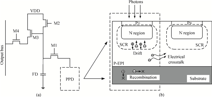
Fig. 1.
Illustration of a 4T pixel with a PPD structure. (a) 4T pixel circuit schematic. (b) Electrical crosstalk mechanism between neighboring PPDs.
SEMICONDUCTOR DEVICES
Chen Cao, Bing Zhang, Xin Li, Longsheng Wu and Junfeng Wang
Corresponding author: Cao Chen, Email:intercaochen@163.com
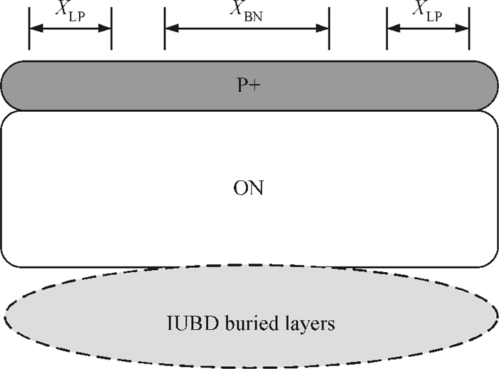
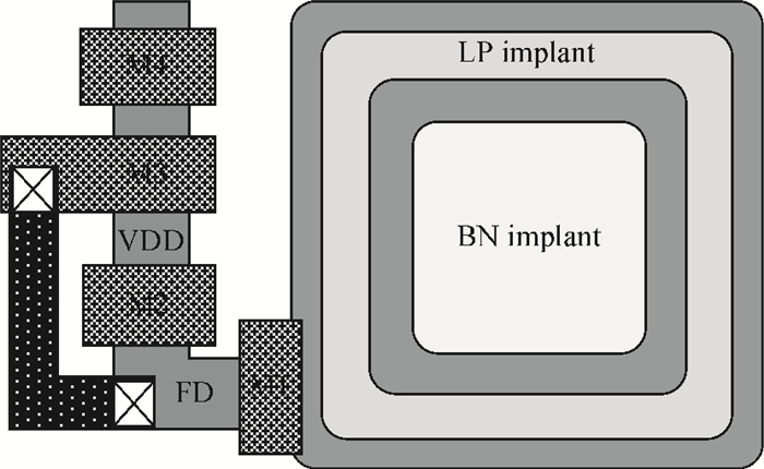
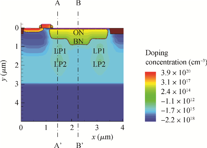
Abstract: A design of an inverse U-shape buried doping in a pinned photodiode (PPD) of CMOS image sensors is proposed for electrical crosstalk suppression between adjacent pixels. The architecture achieves no extra fill factor consumption, and proper built-in electric fields can be established according to the doping gradient created by the injections of the extremely low P-type doping buried regions in the epitaxial layer, causing the excess electrons to easily drift back to the photosensitive area rarely with a diffusion probability; the overall junction capacitance and photosensitive area extensions for a full well capacity (FWC) and internal quantum efficiency (IQE) improving are achieved by the injection of a buried N-type doping. By considering the image lag issue, the process parameters of all the injections have been precisely optimized. Optical simulation results based on the finite difference time domain method show that compared to the conventional PPD, the electrical crosstalk rate of the proposed architecture can be decreased by 60%-80% at an incident wavelength beyond 450 nm, IQE can be clearly improved at an incident wavelength between 400 and 600 nm, and the FWC can be enhanced by 107.5%. Furthermore, the image lag performance is sustained to a perfect low level. The present study provides important guidance on the design of ultra high resolution image sensors.
Keywords: CMOS image sensor, electrical crosstalk, photoelectric performance design, pinned photodiode
| [1] |
Shoushun C, Boussaid F, Bermak A, et al. Robust intermediate readout for deep submicron technology CMOS image sensors. IEEE Sensors J, 2008, 8(3):286 doi: 10.1109/JSEN.2007.912783
|
| [2] |
Han Liqiang, Yao Suying, Xu Jiangtao, et al. Analysis of incomplete charge transfer effects in a CMOS image sensor. Journal of Semiconductors, 2013, 34(5):054009 doi: 10.1088/1674-4926/34/5/054009
|
| [3] |
Li Yiqiang, Li Binqiao, Xu Jiangtao, et al. Charge transfer efficiency improvement of a 4-T pixel by the optimization of electrical potential distribution under the transfer gate. Journal of Semiconductors, 2012, 33(12):124004 doi: 10.1088/1674-4926/33/12/124004
|
| [4] |
Zhang Fudi, Zhang Jianqing, Yang Cui, et al. Performance simulation and architecture optimization for CMOs image sensor pixels scaling down to 1.0μm. IEEE Trans Electron Devices, 2010, 57(4):788 doi: 10.1109/TED.2010.2041858
|
| [5] |
Tsunlai H, Chen Y C. P-sub guard ring design and modeling for the purpose of substrate noise isolation in the SOC era. IEEE Electron Device Lett, 2005, 26(9):693 doi: 10.1109/LED.2005.854351
|
| [6] |
Tseng C H, Wuu S G. Crosstalk improvement technology applicable to 0.14μm CMOS image sensor. IEDM Technical Digest, 2004:997 http://ieeeexplore.com/xpl/articleDetails.jsp?tp=&arnumber=1419356&searchWithin%3Dp_Authors%3A.QT.Shu+Wang.QT.%26pageNumber%3D3%26rowsPerPage%3D75
|
| [7] |
Park B J, Jung J, Moon C R, et al. Deep trench isolation for crosstalk suppression in active pixel sensors with 1.7μm pixel pitch. Jpn J Appl Phys, 2007, 46:2454 doi: 10.1143/JJAP.46.2454
|
| [8] |
Tournier A, Leverd F, Favennec L, et al. Pixel-to-pixel isolation by deep trenchtechnology:application to CMOS image sensor. Proceedings of International Image Sensor Workshop (ⅡSW), 2011:R5 https://www.mendeley.com/research-papers/pixeltopixel-isolation-deep-trench-technology-application-cmos-image-sensor/
|
| [9] |
Michelot J, Roy F, Prima J, et al. Back illuminated vertically pinned photodiode with in depth charge storage. Proceedings of International Image Sensor Workshop (ⅡSW), 2011:R9 http://www.imagesensors.org/Past%20Workshops/2011%20Workshop/2011%20Papers/R09_Michelot_VerticalPPD.pdf
|
| [10] |
Adam G. Investigation of 4T CMOS image sensor design and the effects of radiation damage. PhM Dissertation, University of Surrey, UK, 2010
|
| [11] |
Puliyankot V, Hueting R J. One-dimensional physical model to predict the internal quantum efficiency of Si-based LEDs. IEEE Trans Electron Devices, 2012, 59(1):26 doi: 10.1109/TED.2011.2170992
|
| [12] |
Liu Enke, Zhu Bingsheng, Luo Jinsheng. Semiconductor physics. Beijing:Publishing House of Electronics Industry, 2008(in Chinese)
|
| [13] |
Gunn J B. On carrier accumulation, and the properties of certain semiconductor junctions. Int J Electron, 1958, 4(1):17 doi: 10.1080/00207215808953823?journalCode=tetn19
|
| [14] |
Cao Chen, Zhang Bing, Wu Longsheng, et al. Pinch-off voltage modeling for CMOS image pixels with a pinned photodiode structure. Journal of Semiconductors, 2014, 35(7):074012 doi: 10.1088/1674-4926/35/7/074012
|
| [15] |
Zeng Huiming, Wei Tingcun, Zheng Ran, et al. Modeling of pinned photodiode for CMOS image sensor. IEEE International Conference on Signal Processing, Communications and Computing (ICSPCC), 2011:1 http://ieeexplore.ieee.org/document/6061574/
|
| [16] |
Xiao Hong. Introduction to semiconductor manufacturing technology. Beijing:Publishing House of Electronics Industry, 2013(in Chinese)
|
| [17] |
Synopsys TCAD Tools. http://www.synopsys.com/Tools/TCAD
|
| [18] |
Sun Yu, Zhang Ping, Xu Jiangtao, et al. Full well capacity and quantum efficiency optimization for small size backside illuminated CMOS image pixels with a new photodiode structure. Journal of Semiconductors, 2012, 33(12):124006 doi: 10.1088/1674-4926/33/12/124006
|
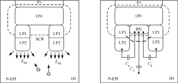
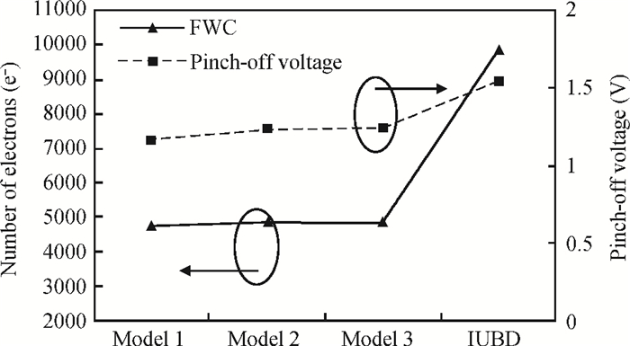
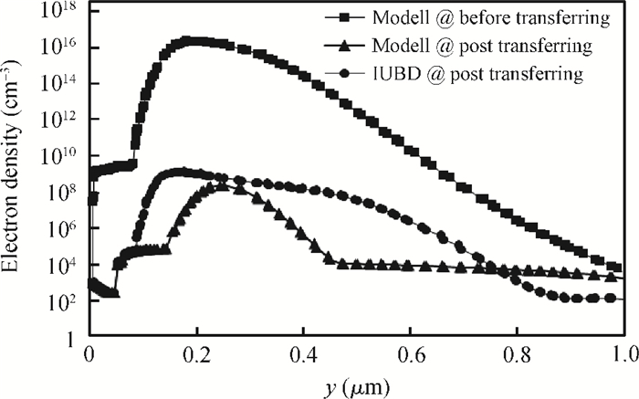
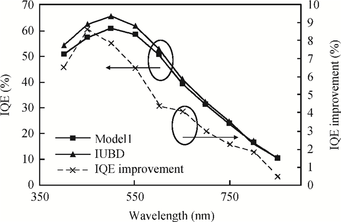
Table 1. Technology flow and process parameters for IUBD architecture implementation.

|
Table 2. Summary of the studied device models.

|
Table 3. Comparison of the conventional and IUBD design.

|
Table 4. Comparison of the proposed IUBD and DTI design.

|
| [1] |
Shoushun C, Boussaid F, Bermak A, et al. Robust intermediate readout for deep submicron technology CMOS image sensors. IEEE Sensors J, 2008, 8(3):286 doi: 10.1109/JSEN.2007.912783
|
| [2] |
Han Liqiang, Yao Suying, Xu Jiangtao, et al. Analysis of incomplete charge transfer effects in a CMOS image sensor. Journal of Semiconductors, 2013, 34(5):054009 doi: 10.1088/1674-4926/34/5/054009
|
| [3] |
Li Yiqiang, Li Binqiao, Xu Jiangtao, et al. Charge transfer efficiency improvement of a 4-T pixel by the optimization of electrical potential distribution under the transfer gate. Journal of Semiconductors, 2012, 33(12):124004 doi: 10.1088/1674-4926/33/12/124004
|
| [4] |
Zhang Fudi, Zhang Jianqing, Yang Cui, et al. Performance simulation and architecture optimization for CMOs image sensor pixels scaling down to 1.0μm. IEEE Trans Electron Devices, 2010, 57(4):788 doi: 10.1109/TED.2010.2041858
|
| [5] |
Tsunlai H, Chen Y C. P-sub guard ring design and modeling for the purpose of substrate noise isolation in the SOC era. IEEE Electron Device Lett, 2005, 26(9):693 doi: 10.1109/LED.2005.854351
|
| [6] |
Tseng C H, Wuu S G. Crosstalk improvement technology applicable to 0.14μm CMOS image sensor. IEDM Technical Digest, 2004:997 http://ieeeexplore.com/xpl/articleDetails.jsp?tp=&arnumber=1419356&searchWithin%3Dp_Authors%3A.QT.Shu+Wang.QT.%26pageNumber%3D3%26rowsPerPage%3D75
|
| [7] |
Park B J, Jung J, Moon C R, et al. Deep trench isolation for crosstalk suppression in active pixel sensors with 1.7μm pixel pitch. Jpn J Appl Phys, 2007, 46:2454 doi: 10.1143/JJAP.46.2454
|
| [8] |
Tournier A, Leverd F, Favennec L, et al. Pixel-to-pixel isolation by deep trenchtechnology:application to CMOS image sensor. Proceedings of International Image Sensor Workshop (ⅡSW), 2011:R5 https://www.mendeley.com/research-papers/pixeltopixel-isolation-deep-trench-technology-application-cmos-image-sensor/
|
| [9] |
Michelot J, Roy F, Prima J, et al. Back illuminated vertically pinned photodiode with in depth charge storage. Proceedings of International Image Sensor Workshop (ⅡSW), 2011:R9 http://www.imagesensors.org/Past%20Workshops/2011%20Workshop/2011%20Papers/R09_Michelot_VerticalPPD.pdf
|
| [10] |
Adam G. Investigation of 4T CMOS image sensor design and the effects of radiation damage. PhM Dissertation, University of Surrey, UK, 2010
|
| [11] |
Puliyankot V, Hueting R J. One-dimensional physical model to predict the internal quantum efficiency of Si-based LEDs. IEEE Trans Electron Devices, 2012, 59(1):26 doi: 10.1109/TED.2011.2170992
|
| [12] |
Liu Enke, Zhu Bingsheng, Luo Jinsheng. Semiconductor physics. Beijing:Publishing House of Electronics Industry, 2008(in Chinese)
|
| [13] |
Gunn J B. On carrier accumulation, and the properties of certain semiconductor junctions. Int J Electron, 1958, 4(1):17 doi: 10.1080/00207215808953823?journalCode=tetn19
|
| [14] |
Cao Chen, Zhang Bing, Wu Longsheng, et al. Pinch-off voltage modeling for CMOS image pixels with a pinned photodiode structure. Journal of Semiconductors, 2014, 35(7):074012 doi: 10.1088/1674-4926/35/7/074012
|
| [15] |
Zeng Huiming, Wei Tingcun, Zheng Ran, et al. Modeling of pinned photodiode for CMOS image sensor. IEEE International Conference on Signal Processing, Communications and Computing (ICSPCC), 2011:1 http://ieeexplore.ieee.org/document/6061574/
|
| [16] |
Xiao Hong. Introduction to semiconductor manufacturing technology. Beijing:Publishing House of Electronics Industry, 2013(in Chinese)
|
| [17] |
Synopsys TCAD Tools. http://www.synopsys.com/Tools/TCAD
|
| [18] |
Sun Yu, Zhang Ping, Xu Jiangtao, et al. Full well capacity and quantum efficiency optimization for small size backside illuminated CMOS image pixels with a new photodiode structure. Journal of Semiconductors, 2012, 33(12):124006 doi: 10.1088/1674-4926/33/12/124006
|


Article views: 3113 Times PDF downloads: 54 Times Cited by: 0 Times
Received: 26 April 2014 Revised: 04 June 2014 Online: Published: 01 November 2014
| Citation: |
Chen Cao, Bing Zhang, Xin Li, Longsheng Wu, Junfeng Wang. Photoelectric characteristics of an inverse U-shape buried doping design for crosstalk suppression in pinned photodiodes[J]. Journal of Semiconductors, 2014, 35(11): 114009. doi: 10.1088/1674-4926/35/11/114009
****
C Cao, B Zhang, X Li, L S Wu, J F Wang. Photoelectric characteristics of an inverse U-shape buried doping design for crosstalk suppression in pinned photodiodes[J]. J. Semicond., 2014, 35(11): 114009. doi: 10.1088/1674-4926/35/11/114009.

|
| [1] |
Shoushun C, Boussaid F, Bermak A, et al. Robust intermediate readout for deep submicron technology CMOS image sensors. IEEE Sensors J, 2008, 8(3):286 doi: 10.1109/JSEN.2007.912783
|
| [2] |
Han Liqiang, Yao Suying, Xu Jiangtao, et al. Analysis of incomplete charge transfer effects in a CMOS image sensor. Journal of Semiconductors, 2013, 34(5):054009 doi: 10.1088/1674-4926/34/5/054009
|
| [3] |
Li Yiqiang, Li Binqiao, Xu Jiangtao, et al. Charge transfer efficiency improvement of a 4-T pixel by the optimization of electrical potential distribution under the transfer gate. Journal of Semiconductors, 2012, 33(12):124004 doi: 10.1088/1674-4926/33/12/124004
|
| [4] |
Zhang Fudi, Zhang Jianqing, Yang Cui, et al. Performance simulation and architecture optimization for CMOs image sensor pixels scaling down to 1.0μm. IEEE Trans Electron Devices, 2010, 57(4):788 doi: 10.1109/TED.2010.2041858
|
| [5] |
Tsunlai H, Chen Y C. P-sub guard ring design and modeling for the purpose of substrate noise isolation in the SOC era. IEEE Electron Device Lett, 2005, 26(9):693 doi: 10.1109/LED.2005.854351
|
| [6] |
Tseng C H, Wuu S G. Crosstalk improvement technology applicable to 0.14μm CMOS image sensor. IEDM Technical Digest, 2004:997 http://ieeeexplore.com/xpl/articleDetails.jsp?tp=&arnumber=1419356&searchWithin%3Dp_Authors%3A.QT.Shu+Wang.QT.%26pageNumber%3D3%26rowsPerPage%3D75
|
| [7] |
Park B J, Jung J, Moon C R, et al. Deep trench isolation for crosstalk suppression in active pixel sensors with 1.7μm pixel pitch. Jpn J Appl Phys, 2007, 46:2454 doi: 10.1143/JJAP.46.2454
|
| [8] |
Tournier A, Leverd F, Favennec L, et al. Pixel-to-pixel isolation by deep trenchtechnology:application to CMOS image sensor. Proceedings of International Image Sensor Workshop (ⅡSW), 2011:R5 https://www.mendeley.com/research-papers/pixeltopixel-isolation-deep-trench-technology-application-cmos-image-sensor/
|
| [9] |
Michelot J, Roy F, Prima J, et al. Back illuminated vertically pinned photodiode with in depth charge storage. Proceedings of International Image Sensor Workshop (ⅡSW), 2011:R9 http://www.imagesensors.org/Past%20Workshops/2011%20Workshop/2011%20Papers/R09_Michelot_VerticalPPD.pdf
|
| [10] |
Adam G. Investigation of 4T CMOS image sensor design and the effects of radiation damage. PhM Dissertation, University of Surrey, UK, 2010
|
| [11] |
Puliyankot V, Hueting R J. One-dimensional physical model to predict the internal quantum efficiency of Si-based LEDs. IEEE Trans Electron Devices, 2012, 59(1):26 doi: 10.1109/TED.2011.2170992
|
| [12] |
Liu Enke, Zhu Bingsheng, Luo Jinsheng. Semiconductor physics. Beijing:Publishing House of Electronics Industry, 2008(in Chinese)
|
| [13] |
Gunn J B. On carrier accumulation, and the properties of certain semiconductor junctions. Int J Electron, 1958, 4(1):17 doi: 10.1080/00207215808953823?journalCode=tetn19
|
| [14] |
Cao Chen, Zhang Bing, Wu Longsheng, et al. Pinch-off voltage modeling for CMOS image pixels with a pinned photodiode structure. Journal of Semiconductors, 2014, 35(7):074012 doi: 10.1088/1674-4926/35/7/074012
|
| [15] |
Zeng Huiming, Wei Tingcun, Zheng Ran, et al. Modeling of pinned photodiode for CMOS image sensor. IEEE International Conference on Signal Processing, Communications and Computing (ICSPCC), 2011:1 http://ieeexplore.ieee.org/document/6061574/
|
| [16] |
Xiao Hong. Introduction to semiconductor manufacturing technology. Beijing:Publishing House of Electronics Industry, 2013(in Chinese)
|
| [17] |
Synopsys TCAD Tools. http://www.synopsys.com/Tools/TCAD
|
| [18] |
Sun Yu, Zhang Ping, Xu Jiangtao, et al. Full well capacity and quantum efficiency optimization for small size backside illuminated CMOS image pixels with a new photodiode structure. Journal of Semiconductors, 2012, 33(12):124006 doi: 10.1088/1674-4926/33/12/124006
|

 WeChat ID
Journal of Semiconductors © 2017 All Rights Reserved 京ICP备05085259号-2

 DownLoad: