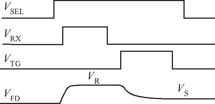
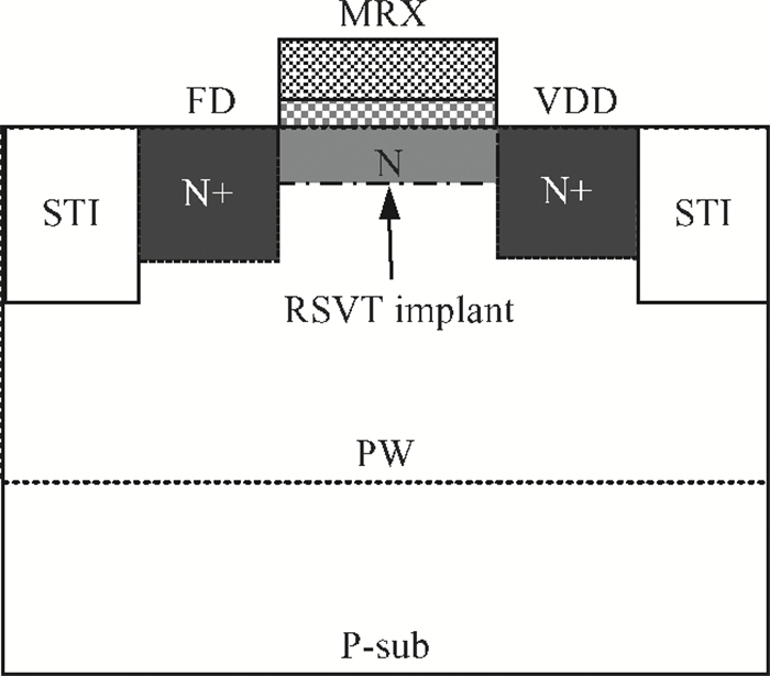
Fig. 1.
(a) Schematic cross-sectional diagram of a typical 4T pixel and (b) the equivalent circuit of lateral transfer in a PPD.
SEMICONDUCTOR DEVICES
Zhongxiang Cao, Quanliang Li, Ye Han, Qi Qin, Peng Feng, Liyuan Liu and Nanjian Wu
Corresponding author: Wu Nanjian, Email:nanjian@semi.ac.cn
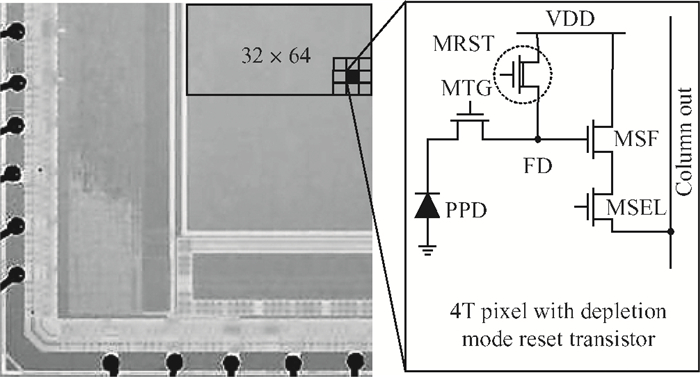
Abstract: This paper proposes pixel process techniques to reduce the charge transfer time in high speed CMOS image sensors. These techniques increase the lateral conductivity of the photo-generated carriers in a pinned photodiode (PPD) and the voltage difference between the PPD and the floating diffusion (FD) node by controlling and optimizing the N doping concentration in the PPD and the threshold voltage of the reset transistor, respectively. The techniques shorten the charge transfer time from the PPD diode to the FD node effectively. The proposed process techniques do not need extra masks and do not cause harm to the fill factor. A sub array of 32×64 pixels was designed and implemented in the 0.18 μm CIS process with five implantation conditions splitting the N region in the PPD. The simulation and measured results demonstrate that the charge transfer time can be decreased by using the proposed techniques. Comparing the charge transfer time of the pixel with the different implantation conditions of the N region, the charge transfer time of 0.32 μs is achieved and 31% of image lag was reduced by using the proposed process techniques.
Keywords: CMOS image sensors, high speed, large-area pinned photodiode, charge transfer time, doping concentration, depletion mode transistor
| [1] |
Theuwissen A J P. CMOS image sensors:state-of-the-art. Solid-State Electron, 2008, 52(9):1403 http://www.sciencedirect.com/science/article/pii/S0038110108001317
|
| [2] |
Xu Jiangtao, Yao Suying, Li Binqiao, et al. Design, analysis, and optimization of a CMOS active pixel sensor. Journal of Semiconductors, 2006, 27(9):1548 http://www.jos.ac.cn/bdtxbcn/ch/reader/view_abstract.aspx?flag=1&file_no=20060906&journal_id=bdtxbcn
|
| [3] |
Li Binqiao, Sun Zhongyan, Xu Jiangtao. Wide dynamic range CMOS image sensor with in-pixel double-exposure and synthesis. Journal of Semiconductors, 2010, 31(5):055002 doi: 10.1088/1674-4926/31/5/055002
|
| [4] |
Li Binqiao, Xu Jiangtao, Xie Shuang, et al. Reset noise reduction through column-level feedback reset in CMOS image sensors. Journal of Semiconductors, 2011, 32(2):025012 doi: 10.1088/1674-4926/32/2/025012
|
| [5] |
Xu Chao, Yao Suying, Xu Jiangtao, et al. A dynamic range extension scheme applied to a TDI CMOS image sensor. Journal of Semiconductors, 2014, 35(2):024013 doi: 10.1088/1674-4926/35/2/024013
|
| [6] |
Fossum E R, Hondongwa D B. A review of the pinned photodiode for CCD and CMOS image sensors. IEEE J Electron Devices Society, 2014, 2(3):33 doi: 10.1109/JEDS.2014.2306412
|
| [7] |
Bhumjae S, Sangsik P, Hyuntaek S. The effect of photodiode shape on charge transfer in CMOS image sensors. Solid-State Electron, 2010, 11:1416 http://www.sciencedirect.com/science/article/pii/S0038110110002224
|
| [8] |
Xu Y, Theuwissen A J P. Image lag analysis and photodiode shape optimization of 4T CMOS pixels. ⅡSW, 2013:153 http://imagesensors.org/Past%20Workshops/2013%20Workshop/2013%20Papers/05-19_Xu_REVISION.pdf
|
| [9] |
Etoh G T, Poggemann D, Kreider, et al. An image sensor which captures 100 consecutive frames at 1000000 frames/s. IEEE Trans Electron Devices, 2003, 50(1):144 doi: 10.1109/TED.2002.806474
|
| [10] |
Takeshita H, Sawada T, Iida T, et al. High-speed charge transfer pinned-photodiode for a CMOS time-of-flight range image sensor. Proc SPIE, 2010, 7536:75360R doi: 10.1117/12.846277
|
| [11] |
Crooks J, Marsh B, Turchetta R, et al. Ultra-high speed imaging at megaframes per second with a megapixel CMOS image sensor. Proc International Image Sensor Workshop, 2013:369 http://www.imagesensors.org/Past%20Workshops/2013%20Workshop/2013%20Papers/11-02_Turchetta_REVISION.pdf
|
| [12] |
Daniel D, Andreas S, Rana M, et al. Lateral drift-field photodiode for low noise, high-speed, large photoactive-area CMOS imaging applications. Nuclear Instruments and Methods in Physics Research Section A:Accelerators, Spectrometers, Detectors and Associated Equipment, 2010, 624(2):470 http://www.sciencedirect.com/science/article/pii/S0168900210007886
|
| [13] |
Kosonocky F W, Yang G, Kabra K R, et al. 360×360 element three-phase very high frame rate burst image sensor:design, operation, and performance. IEEE Trans Electron Devices, 1997, 44(10):1617 doi: 10.1109/16.628813
|
| [14] |
Monoi M, Sasaki S, Dobashi K, et al. A single region CCD image sensor with wide gap electrode and gradual potential channel. Proc SPIE, 2009, 7249:72490I http://adsabs.harvard.edu/abs/2009SPIE.7249E..12M
|
| [15] |
Li Weiping, Xu Jiangtao, Xu Chao, et al. Collection efficiency and charge transfer optimization for a 4-T pixel with multi n-type implants. Journal of Semiconductors, 2011, 32(12):124008 doi: 10.1088/1674-4926/32/12/124008
|
| [16] |
Yonemoto K, Hirofumi S. A numerical analysis of a CMOS image sensor with a simple fixed-pattern-noise-reduction technology. IEEE Trans Electron Devices, 2002, 49(5):746 doi: 10.1109/16.998580
|
| [17] |
Inoue I, Tanaka N, Yamashita H, et al. Low-leakage-current and low-operating-voltage buried photodiode for a CMOS imager. IEEE Trans Electron Devices, 2003, 50(1):43 doi: 10.1109/TED.2002.807525
|
| [18] |
Zhou Yangfan, Cao Zhongxiang, Li Quangliang, et al. Images lag optimization of four-transistor pixel for high speed CMOS image. International Symposium on Photoelectronic Detection and Imaging, 2011:819435 http://proceedings.spiedigitallibrary.org/proceeding.aspx?articleid=1343854
|
| [19] |
Li Yiqiang, Li Binqiao, Xu Jiangtao, et al. Charge transfer efficiency improvement of a 4-T pixel by the optimization of electrical potential distribution under the transfer gate. Journal of Semiconductors, 2012, 33(12):124004 doi: 10.1088/1674-4926/33/12/124004
|
| [20] |
Ramaswami S, Agwani S, Loh L, et al. Characterization of pixel response time and image lag in CMOS sensors. Image Capture Operation, Motorola Inc, Chandler, AZ, 2001:24 http://www.imagesensors.org/Past%20Workshops/2001%20Workshop/2001%20Papers/pg%20110%20Ramaswami.pdf
|
| [21] |
Krymski A, Konstantin F. Estimates for scaling of pinned photodiodes. IEEE Workshop in CCD and Advanced Image Sensors, 2005 http://www.alexima.com/pub/Scaling_Pinned.pdf
|
| [22] |
Neamen D A, Boris P. Semiconductor physics and devices: basic principles. Vol. 3. New York: McGraw-Hill, 2003
|
| [23] |
Fife K, El Gamal A, Wong H S P. A 0.5μm pixel frame-transfer CCD image sensor in 110 nm CMOS. IEEE International Electron Devices Meeting, 2007 http://ieeexplore.ieee.org/xpls/abs_all.jsp?arnumber=4419124
|
| [24] |
Xu Chao, Xu Jiangtao, Yao Suying, et al. Design and optimization of four-transistor pixel for low image lag CMOS image sensor. Proc SPIE, 2013 http://proceedings.spiedigitallibrary.org/proceeding.aspx?articleid=1737646
|
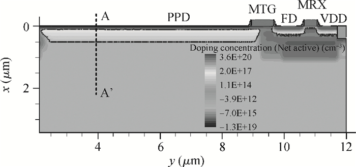
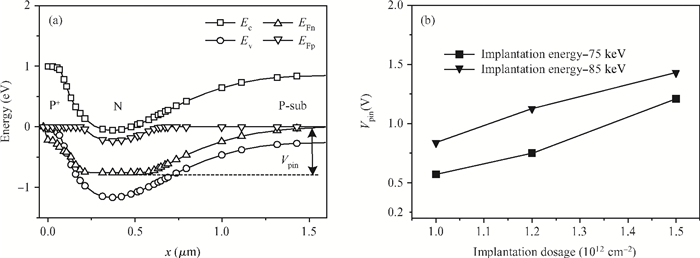

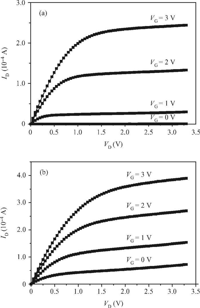
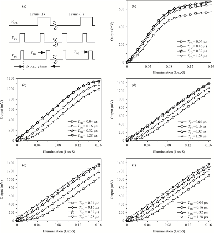
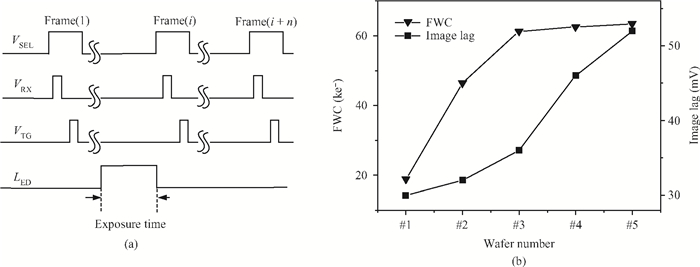
Table 1. Implant conditions of 5 fabricated wafers.

|
| [1] |
Theuwissen A J P. CMOS image sensors:state-of-the-art. Solid-State Electron, 2008, 52(9):1403 http://www.sciencedirect.com/science/article/pii/S0038110108001317
|
| [2] |
Xu Jiangtao, Yao Suying, Li Binqiao, et al. Design, analysis, and optimization of a CMOS active pixel sensor. Journal of Semiconductors, 2006, 27(9):1548 http://www.jos.ac.cn/bdtxbcn/ch/reader/view_abstract.aspx?flag=1&file_no=20060906&journal_id=bdtxbcn
|
| [3] |
Li Binqiao, Sun Zhongyan, Xu Jiangtao. Wide dynamic range CMOS image sensor with in-pixel double-exposure and synthesis. Journal of Semiconductors, 2010, 31(5):055002 doi: 10.1088/1674-4926/31/5/055002
|
| [4] |
Li Binqiao, Xu Jiangtao, Xie Shuang, et al. Reset noise reduction through column-level feedback reset in CMOS image sensors. Journal of Semiconductors, 2011, 32(2):025012 doi: 10.1088/1674-4926/32/2/025012
|
| [5] |
Xu Chao, Yao Suying, Xu Jiangtao, et al. A dynamic range extension scheme applied to a TDI CMOS image sensor. Journal of Semiconductors, 2014, 35(2):024013 doi: 10.1088/1674-4926/35/2/024013
|
| [6] |
Fossum E R, Hondongwa D B. A review of the pinned photodiode for CCD and CMOS image sensors. IEEE J Electron Devices Society, 2014, 2(3):33 doi: 10.1109/JEDS.2014.2306412
|
| [7] |
Bhumjae S, Sangsik P, Hyuntaek S. The effect of photodiode shape on charge transfer in CMOS image sensors. Solid-State Electron, 2010, 11:1416 http://www.sciencedirect.com/science/article/pii/S0038110110002224
|
| [8] |
Xu Y, Theuwissen A J P. Image lag analysis and photodiode shape optimization of 4T CMOS pixels. ⅡSW, 2013:153 http://imagesensors.org/Past%20Workshops/2013%20Workshop/2013%20Papers/05-19_Xu_REVISION.pdf
|
| [9] |
Etoh G T, Poggemann D, Kreider, et al. An image sensor which captures 100 consecutive frames at 1000000 frames/s. IEEE Trans Electron Devices, 2003, 50(1):144 doi: 10.1109/TED.2002.806474
|
| [10] |
Takeshita H, Sawada T, Iida T, et al. High-speed charge transfer pinned-photodiode for a CMOS time-of-flight range image sensor. Proc SPIE, 2010, 7536:75360R doi: 10.1117/12.846277
|
| [11] |
Crooks J, Marsh B, Turchetta R, et al. Ultra-high speed imaging at megaframes per second with a megapixel CMOS image sensor. Proc International Image Sensor Workshop, 2013:369 http://www.imagesensors.org/Past%20Workshops/2013%20Workshop/2013%20Papers/11-02_Turchetta_REVISION.pdf
|
| [12] |
Daniel D, Andreas S, Rana M, et al. Lateral drift-field photodiode for low noise, high-speed, large photoactive-area CMOS imaging applications. Nuclear Instruments and Methods in Physics Research Section A:Accelerators, Spectrometers, Detectors and Associated Equipment, 2010, 624(2):470 http://www.sciencedirect.com/science/article/pii/S0168900210007886
|
| [13] |
Kosonocky F W, Yang G, Kabra K R, et al. 360×360 element three-phase very high frame rate burst image sensor:design, operation, and performance. IEEE Trans Electron Devices, 1997, 44(10):1617 doi: 10.1109/16.628813
|
| [14] |
Monoi M, Sasaki S, Dobashi K, et al. A single region CCD image sensor with wide gap electrode and gradual potential channel. Proc SPIE, 2009, 7249:72490I http://adsabs.harvard.edu/abs/2009SPIE.7249E..12M
|
| [15] |
Li Weiping, Xu Jiangtao, Xu Chao, et al. Collection efficiency and charge transfer optimization for a 4-T pixel with multi n-type implants. Journal of Semiconductors, 2011, 32(12):124008 doi: 10.1088/1674-4926/32/12/124008
|
| [16] |
Yonemoto K, Hirofumi S. A numerical analysis of a CMOS image sensor with a simple fixed-pattern-noise-reduction technology. IEEE Trans Electron Devices, 2002, 49(5):746 doi: 10.1109/16.998580
|
| [17] |
Inoue I, Tanaka N, Yamashita H, et al. Low-leakage-current and low-operating-voltage buried photodiode for a CMOS imager. IEEE Trans Electron Devices, 2003, 50(1):43 doi: 10.1109/TED.2002.807525
|
| [18] |
Zhou Yangfan, Cao Zhongxiang, Li Quangliang, et al. Images lag optimization of four-transistor pixel for high speed CMOS image. International Symposium on Photoelectronic Detection and Imaging, 2011:819435 http://proceedings.spiedigitallibrary.org/proceeding.aspx?articleid=1343854
|
| [19] |
Li Yiqiang, Li Binqiao, Xu Jiangtao, et al. Charge transfer efficiency improvement of a 4-T pixel by the optimization of electrical potential distribution under the transfer gate. Journal of Semiconductors, 2012, 33(12):124004 doi: 10.1088/1674-4926/33/12/124004
|
| [20] |
Ramaswami S, Agwani S, Loh L, et al. Characterization of pixel response time and image lag in CMOS sensors. Image Capture Operation, Motorola Inc, Chandler, AZ, 2001:24 http://www.imagesensors.org/Past%20Workshops/2001%20Workshop/2001%20Papers/pg%20110%20Ramaswami.pdf
|
| [21] |
Krymski A, Konstantin F. Estimates for scaling of pinned photodiodes. IEEE Workshop in CCD and Advanced Image Sensors, 2005 http://www.alexima.com/pub/Scaling_Pinned.pdf
|
| [22] |
Neamen D A, Boris P. Semiconductor physics and devices: basic principles. Vol. 3. New York: McGraw-Hill, 2003
|
| [23] |
Fife K, El Gamal A, Wong H S P. A 0.5μm pixel frame-transfer CCD image sensor in 110 nm CMOS. IEEE International Electron Devices Meeting, 2007 http://ieeexplore.ieee.org/xpls/abs_all.jsp?arnumber=4419124
|
| [24] |
Xu Chao, Xu Jiangtao, Yao Suying, et al. Design and optimization of four-transistor pixel for low image lag CMOS image sensor. Proc SPIE, 2013 http://proceedings.spiedigitallibrary.org/proceeding.aspx?articleid=1737646
|


Article views: 3747 Times PDF downloads: 117 Times Cited by: 0 Times
Received: 05 May 2014 Revised: 21 May 2014 Online: Published: 01 November 2014
| Citation: |
Zhongxiang Cao, Quanliang Li, Ye Han, Qi Qin, Peng Feng, Liyuan Liu, Nanjian Wu. Process techniques of charge transfer time reduction for high speed CMOS image sensors[J]. Journal of Semiconductors, 2014, 35(11): 114010. doi: 10.1088/1674-4926/35/11/114010
****
Z X Cao, Q L Li, Y Han, Q Qin, P Feng, L Y Liu, N J Wu. Process techniques of charge transfer time reduction for high speed CMOS image sensors[J]. J. Semicond., 2014, 35(11): 114010. doi: 10.1088/1674-4926/35/11/114010.

|
| [1] |
Theuwissen A J P. CMOS image sensors:state-of-the-art. Solid-State Electron, 2008, 52(9):1403 http://www.sciencedirect.com/science/article/pii/S0038110108001317
|
| [2] |
Xu Jiangtao, Yao Suying, Li Binqiao, et al. Design, analysis, and optimization of a CMOS active pixel sensor. Journal of Semiconductors, 2006, 27(9):1548 http://www.jos.ac.cn/bdtxbcn/ch/reader/view_abstract.aspx?flag=1&file_no=20060906&journal_id=bdtxbcn
|
| [3] |
Li Binqiao, Sun Zhongyan, Xu Jiangtao. Wide dynamic range CMOS image sensor with in-pixel double-exposure and synthesis. Journal of Semiconductors, 2010, 31(5):055002 doi: 10.1088/1674-4926/31/5/055002
|
| [4] |
Li Binqiao, Xu Jiangtao, Xie Shuang, et al. Reset noise reduction through column-level feedback reset in CMOS image sensors. Journal of Semiconductors, 2011, 32(2):025012 doi: 10.1088/1674-4926/32/2/025012
|
| [5] |
Xu Chao, Yao Suying, Xu Jiangtao, et al. A dynamic range extension scheme applied to a TDI CMOS image sensor. Journal of Semiconductors, 2014, 35(2):024013 doi: 10.1088/1674-4926/35/2/024013
|
| [6] |
Fossum E R, Hondongwa D B. A review of the pinned photodiode for CCD and CMOS image sensors. IEEE J Electron Devices Society, 2014, 2(3):33 doi: 10.1109/JEDS.2014.2306412
|
| [7] |
Bhumjae S, Sangsik P, Hyuntaek S. The effect of photodiode shape on charge transfer in CMOS image sensors. Solid-State Electron, 2010, 11:1416 http://www.sciencedirect.com/science/article/pii/S0038110110002224
|
| [8] |
Xu Y, Theuwissen A J P. Image lag analysis and photodiode shape optimization of 4T CMOS pixels. ⅡSW, 2013:153 http://imagesensors.org/Past%20Workshops/2013%20Workshop/2013%20Papers/05-19_Xu_REVISION.pdf
|
| [9] |
Etoh G T, Poggemann D, Kreider, et al. An image sensor which captures 100 consecutive frames at 1000000 frames/s. IEEE Trans Electron Devices, 2003, 50(1):144 doi: 10.1109/TED.2002.806474
|
| [10] |
Takeshita H, Sawada T, Iida T, et al. High-speed charge transfer pinned-photodiode for a CMOS time-of-flight range image sensor. Proc SPIE, 2010, 7536:75360R doi: 10.1117/12.846277
|
| [11] |
Crooks J, Marsh B, Turchetta R, et al. Ultra-high speed imaging at megaframes per second with a megapixel CMOS image sensor. Proc International Image Sensor Workshop, 2013:369 http://www.imagesensors.org/Past%20Workshops/2013%20Workshop/2013%20Papers/11-02_Turchetta_REVISION.pdf
|
| [12] |
Daniel D, Andreas S, Rana M, et al. Lateral drift-field photodiode for low noise, high-speed, large photoactive-area CMOS imaging applications. Nuclear Instruments and Methods in Physics Research Section A:Accelerators, Spectrometers, Detectors and Associated Equipment, 2010, 624(2):470 http://www.sciencedirect.com/science/article/pii/S0168900210007886
|
| [13] |
Kosonocky F W, Yang G, Kabra K R, et al. 360×360 element three-phase very high frame rate burst image sensor:design, operation, and performance. IEEE Trans Electron Devices, 1997, 44(10):1617 doi: 10.1109/16.628813
|
| [14] |
Monoi M, Sasaki S, Dobashi K, et al. A single region CCD image sensor with wide gap electrode and gradual potential channel. Proc SPIE, 2009, 7249:72490I http://adsabs.harvard.edu/abs/2009SPIE.7249E..12M
|
| [15] |
Li Weiping, Xu Jiangtao, Xu Chao, et al. Collection efficiency and charge transfer optimization for a 4-T pixel with multi n-type implants. Journal of Semiconductors, 2011, 32(12):124008 doi: 10.1088/1674-4926/32/12/124008
|
| [16] |
Yonemoto K, Hirofumi S. A numerical analysis of a CMOS image sensor with a simple fixed-pattern-noise-reduction technology. IEEE Trans Electron Devices, 2002, 49(5):746 doi: 10.1109/16.998580
|
| [17] |
Inoue I, Tanaka N, Yamashita H, et al. Low-leakage-current and low-operating-voltage buried photodiode for a CMOS imager. IEEE Trans Electron Devices, 2003, 50(1):43 doi: 10.1109/TED.2002.807525
|
| [18] |
Zhou Yangfan, Cao Zhongxiang, Li Quangliang, et al. Images lag optimization of four-transistor pixel for high speed CMOS image. International Symposium on Photoelectronic Detection and Imaging, 2011:819435 http://proceedings.spiedigitallibrary.org/proceeding.aspx?articleid=1343854
|
| [19] |
Li Yiqiang, Li Binqiao, Xu Jiangtao, et al. Charge transfer efficiency improvement of a 4-T pixel by the optimization of electrical potential distribution under the transfer gate. Journal of Semiconductors, 2012, 33(12):124004 doi: 10.1088/1674-4926/33/12/124004
|
| [20] |
Ramaswami S, Agwani S, Loh L, et al. Characterization of pixel response time and image lag in CMOS sensors. Image Capture Operation, Motorola Inc, Chandler, AZ, 2001:24 http://www.imagesensors.org/Past%20Workshops/2001%20Workshop/2001%20Papers/pg%20110%20Ramaswami.pdf
|
| [21] |
Krymski A, Konstantin F. Estimates for scaling of pinned photodiodes. IEEE Workshop in CCD and Advanced Image Sensors, 2005 http://www.alexima.com/pub/Scaling_Pinned.pdf
|
| [22] |
Neamen D A, Boris P. Semiconductor physics and devices: basic principles. Vol. 3. New York: McGraw-Hill, 2003
|
| [23] |
Fife K, El Gamal A, Wong H S P. A 0.5μm pixel frame-transfer CCD image sensor in 110 nm CMOS. IEEE International Electron Devices Meeting, 2007 http://ieeexplore.ieee.org/xpls/abs_all.jsp?arnumber=4419124
|
| [24] |
Xu Chao, Xu Jiangtao, Yao Suying, et al. Design and optimization of four-transistor pixel for low image lag CMOS image sensor. Proc SPIE, 2013 http://proceedings.spiedigitallibrary.org/proceeding.aspx?articleid=1737646
|

 WeChat ID
Journal of Semiconductors © 2017 All Rights Reserved 京ICP备05085259号-2

 DownLoad: