


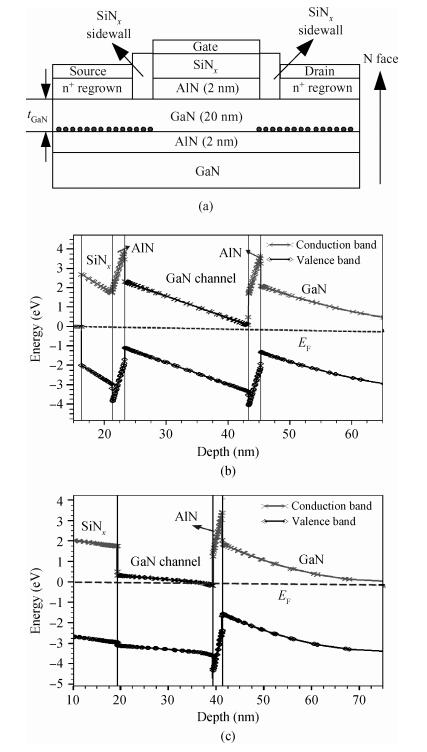
Fig. 1.
(a) Schematic of the device cross section. (b) Band diagram underneath the gate region. (c) Band diagram underneath the SiN$_x$ sidewall access region.
SEMICONDUCTOR DEVICES
Corresponding author: Li Bin, Email:bin_lichina@foxmail.com
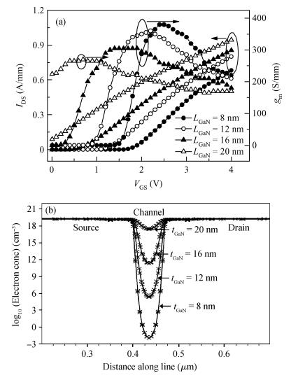
Abstract: This paper aims to simulate the I-V static characteristic of the enhancement-mode (E-mode) N-polar GaN metal-insulator-semiconductor field effect transistor (MISFET) with self-aligned source/drain regions. Firstly, with SILVACO TCAD device simulation, the drain-source current as a function of the gate-source voltage is calculated and the dependence of the drain-source current on the drain-source voltage in the case of different gate-source voltages for the device with a 0.62 μm gate length is investigated. Secondly, a comparison is made with the experimental report. Lastly, the transfer characteristic with different gate lengths and different buffer layers has been performed. The results show that the simulation is in accord with the experiment at the gate length of 0.62 μm and the short channel effect becomes pronounced as gate length decreases. The E-mode will not be held below a 100 nm gate length unless both transversal scaling and vertical scaling are being carried out simultaneously.
Keywords: GaN, enhancement-mode, short channel effect, MISFET
| [1] |
Xu Z X, Zhang W M, Xu F, et al. Investigation of 600 V GaN HEMTs for high efficiency and high temperature applications. Twenty-Ninth Annual IEEE Applied Power Electronics Conference and Exposition (APEC), 2014:131
|
| [2] |
Ramanan N, Lee B, Misra V. Device modeling for understanding AlGaN/GaN HEMT gate-lag. IEEE Trans Electron Devices, 2014, 61(6):2012 doi: 10.1109/TED.2014.2313814
|
| [3] |
Wang J, Sun L L, Jun L, et al. A surface-potential-based model for AlGaN/AlN/GaN HEMT. Journal of Semiconductors, 2013, 34(9):094002 doi: 10.1088/1674-4926/34/9/094002
|
| [4] |
Zhuo X J, Zhang J, Li D W, et al. Enhanced performances of InGaN/GaN-based blue LED with an ultra-thin inserting layer between GaN barriers and InGaN wells. Opt Commun, 2014, 325:129 doi: 10.1016/j.optcom.2014.04.018
|
| [5] |
Martínez-Gutiérrez D, Velasco V R. Transverse acoustic waves in piezoelectric ZnO/MgO and GaN/AlN Fibonacci-periodic superlattices. Surf Sci, 2014, 624:58 doi: 10.1016/j.susc.2014.01.020
|
| [6] |
Zhu Y X, Cao W W, Fan Y Y, et al. Effects of rapid thermal annealing on ohmic contact of AlGaN/GaN HEMTs. Journal of Semiconductors, 2014, 35(2):026004 doi: 10.1088/1674-4926/35/2/026004
|
| [7] |
Kim H, Ryou J H, Dupuis R D, et al. Electrical characteristics of contacts to thin film N-polar n-type GaN. Appl Phys Lett, 2008, 93(19):192106 doi: 10.1063/1.3013838
|
| [8] |
Liu X S, Chen K J. GaN single-polarity power supply bootstrapped comparator for high-temperature electronics. IEEE Trans Electron Device Lett, 2011, 32(1):27 doi: 10.1109/LED.2010.2088376
|
| [9] |
Yuan L, Chen H, Chen K J. Normally off AlGaN/GaN metal 2DEG tunnel-junction field-effect transistors. IEEE Electron Device Lett, 2011, 32(3):303 doi: 10.1109/LED.2010.2095823
|
| [10] |
Im K S, Ha J B, Kim K W, J et al. Normally off GaN MOSFET based on AlGaN/GaN heterostructure with extremely high 2DEG density grown on silicon substrate. IEEE Electron Device Lett, 2011, 31(3):192
|
| [11] |
Ahn H K, Kim Z S, Bae S B, et al. Normally-off dual gate AlGaN/GaN MISFET with selective area-recessed floating gate. Solid-State Electron, 2014, 95:42 doi: 10.1016/j.sse.2014.03.005
|
| [12] |
Song X B, Gu G D, Shao B, et al. DC and RF characteristics of enhancement-mode InAlN/GaN HEMT with fluorine treatment. Journal of Semiconductors, 2014, 35(4):044002 doi: 10.1088/1674-4926/35/4/044002
|
| [13] |
Farahmand M, Garetto C, Bellotti E, et al. Monte Carlo simulation of electron transport in the Ⅲ-nitride wurtzite phase materials system:binaries and ternaries. IEEE Trans Electron Devices, 2001, 48(3):535 doi: 10.1109/16.906448
|
| [14] |
Caridi E A, Chang T Y, Goossen K W, et al. Direct demonstration of a misfit strain-generated electric field in a [111] growth axis zinc-blende heterostructure. Appl Phys Lett, 1990, 56(7):659 doi: 10.1063/1.102729
|
| [15] |
Singisetti U, Wong M H, Dasgupta S, et al. Enhancement-mode N-polar GaN MISFETs with self-aligned source/drain regrowth. IEEE Electron Device Lett, 2011, 32(2):137 doi: 10.1109/LED.2010.2090125
|
| [16] |
ATLAS Device simulation software User's Manual, SILVACO International
|
| [17] |
Albrecht J D, Wang R P, Ruden P P, et al. Electron transport characteristics of GaN for high temperature device modeling. J Appl Phys, 1998, 83(9):4777 doi: 10.1063/1.367269
|
| [18] |
Farahmand M, Garetto C, Bellotti E, et al. Monte Carlo simulation of electron transport in the Ⅲ-nitride wurtzite phase materials system:binaries and ternaries. IEEE Trans Electron Devices, 2001, 48(3):535 doi: 10.1109/16.906448
|
| [19] |
Bernardini F, Fiorentini V, Vanderbilt D. Spontaneous polarization and piezoelectric constants of Ⅲ-Ⅴ nitrides. Phys Rev B, 1997, 56(16):R10024 doi: 10.1103/PhysRevB.56.R10024
|
| [20] |
Ambacher O, Smart J, Shealy J R, et al. Two-dimensional electron gases induced by spontaneous and piezoelectric polarization charges in N-and Ga-face AlGaN/GaN heterostructures. J Appl Phys, 1999, 85(6):3222 doi: 10.1063/1.369664
|
| [21] |
Guerra D, Akis R, Marino F A, et al. Aspect ratio impact on RF and DC performance of state-of-the-art short-channel GaN and InGaAs HEMTs. IEEE Electron Device Lett, 2010, 31(11):1217
|
| [22] |
Jessen G H, Fitch R C, Gillespie J K, et al. Short-channel effect limitations on high-frequency operation of AlGaN/GaN HEMTs for T-gate devices. IEEE Trans Electron Devices, 2007, 54(10):2589 doi: 10.1109/TED.2007.904476
|


Article views: 3509 Times PDF downloads: 13 Times Cited by: 0 Times
Received: 21 April 2014 Revised: 23 June 2014 Online: Published: 01 December 2014
| Citation: |
Bin Li, Lan Wei, Cai Wen. Static characteristics and short channel effect in enhancement-mode AlN/GaN/AlN N-polar MISFET with self-aligned source/drain regions[J]. Journal of Semiconductors, 2014, 35(12): 124006. doi: 10.1088/1674-4926/35/12/124006
****
B Li, L Wei, C Wen. Static characteristics and short channel effect in enhancement-mode AlN/GaN/AlN N-polar MISFET with self-aligned source/drain regions[J]. J. Semicond., 2014, 35(12): 124006. doi: 10.1088/1674-4926/35/12/124006.

|
| [1] |
Xu Z X, Zhang W M, Xu F, et al. Investigation of 600 V GaN HEMTs for high efficiency and high temperature applications. Twenty-Ninth Annual IEEE Applied Power Electronics Conference and Exposition (APEC), 2014:131
|
| [2] |
Ramanan N, Lee B, Misra V. Device modeling for understanding AlGaN/GaN HEMT gate-lag. IEEE Trans Electron Devices, 2014, 61(6):2012 doi: 10.1109/TED.2014.2313814
|
| [3] |
Wang J, Sun L L, Jun L, et al. A surface-potential-based model for AlGaN/AlN/GaN HEMT. Journal of Semiconductors, 2013, 34(9):094002 doi: 10.1088/1674-4926/34/9/094002
|
| [4] |
Zhuo X J, Zhang J, Li D W, et al. Enhanced performances of InGaN/GaN-based blue LED with an ultra-thin inserting layer between GaN barriers and InGaN wells. Opt Commun, 2014, 325:129 doi: 10.1016/j.optcom.2014.04.018
|
| [5] |
Martínez-Gutiérrez D, Velasco V R. Transverse acoustic waves in piezoelectric ZnO/MgO and GaN/AlN Fibonacci-periodic superlattices. Surf Sci, 2014, 624:58 doi: 10.1016/j.susc.2014.01.020
|
| [6] |
Zhu Y X, Cao W W, Fan Y Y, et al. Effects of rapid thermal annealing on ohmic contact of AlGaN/GaN HEMTs. Journal of Semiconductors, 2014, 35(2):026004 doi: 10.1088/1674-4926/35/2/026004
|
| [7] |
Kim H, Ryou J H, Dupuis R D, et al. Electrical characteristics of contacts to thin film N-polar n-type GaN. Appl Phys Lett, 2008, 93(19):192106 doi: 10.1063/1.3013838
|
| [8] |
Liu X S, Chen K J. GaN single-polarity power supply bootstrapped comparator for high-temperature electronics. IEEE Trans Electron Device Lett, 2011, 32(1):27 doi: 10.1109/LED.2010.2088376
|
| [9] |
Yuan L, Chen H, Chen K J. Normally off AlGaN/GaN metal 2DEG tunnel-junction field-effect transistors. IEEE Electron Device Lett, 2011, 32(3):303 doi: 10.1109/LED.2010.2095823
|
| [10] |
Im K S, Ha J B, Kim K W, J et al. Normally off GaN MOSFET based on AlGaN/GaN heterostructure with extremely high 2DEG density grown on silicon substrate. IEEE Electron Device Lett, 2011, 31(3):192
|
| [11] |
Ahn H K, Kim Z S, Bae S B, et al. Normally-off dual gate AlGaN/GaN MISFET with selective area-recessed floating gate. Solid-State Electron, 2014, 95:42 doi: 10.1016/j.sse.2014.03.005
|
| [12] |
Song X B, Gu G D, Shao B, et al. DC and RF characteristics of enhancement-mode InAlN/GaN HEMT with fluorine treatment. Journal of Semiconductors, 2014, 35(4):044002 doi: 10.1088/1674-4926/35/4/044002
|
| [13] |
Farahmand M, Garetto C, Bellotti E, et al. Monte Carlo simulation of electron transport in the Ⅲ-nitride wurtzite phase materials system:binaries and ternaries. IEEE Trans Electron Devices, 2001, 48(3):535 doi: 10.1109/16.906448
|
| [14] |
Caridi E A, Chang T Y, Goossen K W, et al. Direct demonstration of a misfit strain-generated electric field in a [111] growth axis zinc-blende heterostructure. Appl Phys Lett, 1990, 56(7):659 doi: 10.1063/1.102729
|
| [15] |
Singisetti U, Wong M H, Dasgupta S, et al. Enhancement-mode N-polar GaN MISFETs with self-aligned source/drain regrowth. IEEE Electron Device Lett, 2011, 32(2):137 doi: 10.1109/LED.2010.2090125
|
| [16] |
ATLAS Device simulation software User's Manual, SILVACO International
|
| [17] |
Albrecht J D, Wang R P, Ruden P P, et al. Electron transport characteristics of GaN for high temperature device modeling. J Appl Phys, 1998, 83(9):4777 doi: 10.1063/1.367269
|
| [18] |
Farahmand M, Garetto C, Bellotti E, et al. Monte Carlo simulation of electron transport in the Ⅲ-nitride wurtzite phase materials system:binaries and ternaries. IEEE Trans Electron Devices, 2001, 48(3):535 doi: 10.1109/16.906448
|
| [19] |
Bernardini F, Fiorentini V, Vanderbilt D. Spontaneous polarization and piezoelectric constants of Ⅲ-Ⅴ nitrides. Phys Rev B, 1997, 56(16):R10024 doi: 10.1103/PhysRevB.56.R10024
|
| [20] |
Ambacher O, Smart J, Shealy J R, et al. Two-dimensional electron gases induced by spontaneous and piezoelectric polarization charges in N-and Ga-face AlGaN/GaN heterostructures. J Appl Phys, 1999, 85(6):3222 doi: 10.1063/1.369664
|
| [21] |
Guerra D, Akis R, Marino F A, et al. Aspect ratio impact on RF and DC performance of state-of-the-art short-channel GaN and InGaAs HEMTs. IEEE Electron Device Lett, 2010, 31(11):1217
|
| [22] |
Jessen G H, Fitch R C, Gillespie J K, et al. Short-channel effect limitations on high-frequency operation of AlGaN/GaN HEMTs for T-gate devices. IEEE Trans Electron Devices, 2007, 54(10):2589 doi: 10.1109/TED.2007.904476
|

 WeChat ID
Journal of Semiconductors © 2017 All Rights Reserved 京ICP备05085259号-2

 DownLoad:


