


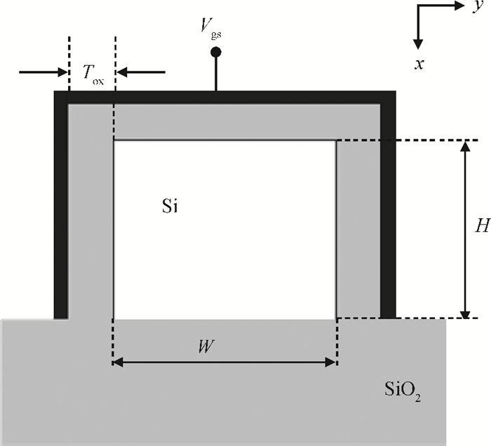
Fig. 1.
Cross section of the silicon tri-gate MOSFETs under study.
SEMICONDUCTOR DEVICES
P. Vimala and N. B. Balamurugan
Corresponding author: P. Vimala, Email:vimalapalanichamy@tce.edu
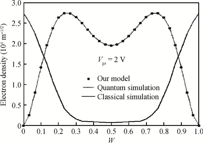
Abstract: Quantum effects are predominant in tri-gate MOSFETs, so a model should be developed. For the first time, this paper presents the analytical model for quantization effects of thin film silicon tri-gate MOSFETs by using variational approach. An analytical expression of the inversion charge distribution function (ICDF) or wave function for the tri-gate MOSFETs has been obtained. This obtained ICDF is used to calculate the important device parameters, such as the inversion charge centroid and inversion charge density. The results are validated against with the simulation data.
Keywords: device modeling, energy quantization, inversion charge density, Poisson-Schrodinger equation, trigate MOSFET
| [1] |
Frank D J, Dennard R H, Nowak E, et al. Device scaling limits of Si MOSFETs and their application dependencies. Proc IEEE, 2001, 89(3):259 doi: 10.1109/5.915374
|
| [2] |
Doyle B, Arghavani R, Barlage D, et al. Transistor elements for 30 nm physical gate lengths and beyond. Intel Technol J, 2002, 6(2):42
|
| [3] |
He J, Liu F, Bian W, et al. An approximate carrier-based compact model for fully depleted surrounding-gate MOSFETs with a finite doping body. Semicond Sci Technol, 2007, 22(6):671 doi: 10.1088/0268-1242/22/6/015
|
| [4] |
Son A, Kim J, Jeong N, et al. Improved explicit current-voltage model for long-channel undoped surrounding-gate metal oxide semiconductor field effect transistor. Jpn J Appl Phys, 2009, 48:412 doi: 10.1143/JJAP.48.04C035/meta
|
| [5] |
Lixin G, Fossum J G. Analytical modeling of quantization and volume inversion in thin Si-film DG MOSFETs. IEEE Trans Electron Devices, 2002, 49(2):287 doi: 10.1109/16.981219
|
| [6] |
Jimenez D, Inguiez B. Continuous analytic Ⅳ model for surrounding-gate MOSFETs. IEEE Electron Device Lett, 2004, 25(8):571 doi: 10.1109/LED.2004.831902
|
| [7] |
Iniguez B, Jimenez D, Roig J, et al. Explicit continuous model for long-channel undoped surrounding-gate MOSFETs. IEEE Trans Electron Devices, 2005, 52(8):1868 doi: 10.1109/TED.2005.852892
|
| [8] |
Colinge J P. FinFETs and other multi-gate MOSFETs. Springer, 2008:49
|
| [9] |
Kranti A, Armstrong G A. Performance assessment of nanoscale double-and triple-gate FinFETs. Semicond Sci Technol, 2006, 21(2):409 doi: 10.1088/0268-1242/21/4/002/meta
|
| [10] |
Jin Y W, Zeng C, Ma L, et al. Analytical threshold voltage model with TCAD simulation verification for design and evalution of tri-gate MOSFETs. Solid-State Electron, 2007, 51:347 doi: 10.1016/j.sse.2007.01.023
|
| [11] |
Tsormpatzoglou A, Dimitriadis C A, Clerc R, et al. Semi analytical modeling of short-channel effects in lightly doped silicon trigate MOSFETs. IEEE Trans Electron Devices, 2008, 55:2623 doi: 10.1109/TED.2008.2003096
|
| [12] |
Tsormpatzoglou A, Tassis D H, Dimitriadis C A, et al. Analytical threshold voltage model for lightly doped short-channel tri-gate MOSFETs. Solid-State Electron, 2011, 57:31 doi: 10.1016/j.sse.2010.10.022
|
| [13] |
Colinge J P, Alderman J C, Xiong W, et al. Quantum mechanical effects in trigate SOI MOSFET. IEEE Trans Electron Devices, 2006, 53(5):1131 doi: 10.1109/TED.2006.871872
|
| [14] |
Granzner R, Thiele S, Schippel C, et al. Quantum effects on the gate capacitance of trigate SOI MOSFETs. IEEE Trans Electron Devices, 2010, 57(12):3231 doi: 10.1109/TED.2010.2077639
|
| [15] |
Juan A, L'opez-Villanueva, Cartujo-Casinello P, et al. Effects of the Inversion layer centroid on MOSFET behaviour. IEEE Trans Electron Devices, 1997, 44(11):1915 doi: 10.1109/16.641361
|
| [16] |
Roldan J B, Godoy A, Gamiz F, et al. Modeling the centroid and the inversion charge in cylindrical surrounding gate MOSFETs, including quantum effects. IEEE Trans Electron Devices, 2008, 55(1):411 doi: 10.1109/TED.2007.911096
|


Article views: 2966 Times PDF downloads: 16 Times Cited by: 0 Times
Received: 22 August 2013 Revised: 29 September 2013 Online: Published: 01 March 2014
| Citation: |
P. Vimala, N. B. Balamurugan. Modeling and simulation of nanoscale tri-gate MOSFETs including quantum effects[J]. Journal of Semiconductors, 2014, 35(3): 034001. doi: 10.1088/1674-4926/35/3/034001
****
P. Vimala, N. B. Balamurugan. Modeling and simulation of nanoscale tri-gate MOSFETs including quantum effects[J]. J. Semicond., 2014, 35(3): 034001. doi: 10.1088/1674-4926/35/3/034001.

|
| [1] |
Frank D J, Dennard R H, Nowak E, et al. Device scaling limits of Si MOSFETs and their application dependencies. Proc IEEE, 2001, 89(3):259 doi: 10.1109/5.915374
|
| [2] |
Doyle B, Arghavani R, Barlage D, et al. Transistor elements for 30 nm physical gate lengths and beyond. Intel Technol J, 2002, 6(2):42
|
| [3] |
He J, Liu F, Bian W, et al. An approximate carrier-based compact model for fully depleted surrounding-gate MOSFETs with a finite doping body. Semicond Sci Technol, 2007, 22(6):671 doi: 10.1088/0268-1242/22/6/015
|
| [4] |
Son A, Kim J, Jeong N, et al. Improved explicit current-voltage model for long-channel undoped surrounding-gate metal oxide semiconductor field effect transistor. Jpn J Appl Phys, 2009, 48:412 doi: 10.1143/JJAP.48.04C035/meta
|
| [5] |
Lixin G, Fossum J G. Analytical modeling of quantization and volume inversion in thin Si-film DG MOSFETs. IEEE Trans Electron Devices, 2002, 49(2):287 doi: 10.1109/16.981219
|
| [6] |
Jimenez D, Inguiez B. Continuous analytic Ⅳ model for surrounding-gate MOSFETs. IEEE Electron Device Lett, 2004, 25(8):571 doi: 10.1109/LED.2004.831902
|
| [7] |
Iniguez B, Jimenez D, Roig J, et al. Explicit continuous model for long-channel undoped surrounding-gate MOSFETs. IEEE Trans Electron Devices, 2005, 52(8):1868 doi: 10.1109/TED.2005.852892
|
| [8] |
Colinge J P. FinFETs and other multi-gate MOSFETs. Springer, 2008:49
|
| [9] |
Kranti A, Armstrong G A. Performance assessment of nanoscale double-and triple-gate FinFETs. Semicond Sci Technol, 2006, 21(2):409 doi: 10.1088/0268-1242/21/4/002/meta
|
| [10] |
Jin Y W, Zeng C, Ma L, et al. Analytical threshold voltage model with TCAD simulation verification for design and evalution of tri-gate MOSFETs. Solid-State Electron, 2007, 51:347 doi: 10.1016/j.sse.2007.01.023
|
| [11] |
Tsormpatzoglou A, Dimitriadis C A, Clerc R, et al. Semi analytical modeling of short-channel effects in lightly doped silicon trigate MOSFETs. IEEE Trans Electron Devices, 2008, 55:2623 doi: 10.1109/TED.2008.2003096
|
| [12] |
Tsormpatzoglou A, Tassis D H, Dimitriadis C A, et al. Analytical threshold voltage model for lightly doped short-channel tri-gate MOSFETs. Solid-State Electron, 2011, 57:31 doi: 10.1016/j.sse.2010.10.022
|
| [13] |
Colinge J P, Alderman J C, Xiong W, et al. Quantum mechanical effects in trigate SOI MOSFET. IEEE Trans Electron Devices, 2006, 53(5):1131 doi: 10.1109/TED.2006.871872
|
| [14] |
Granzner R, Thiele S, Schippel C, et al. Quantum effects on the gate capacitance of trigate SOI MOSFETs. IEEE Trans Electron Devices, 2010, 57(12):3231 doi: 10.1109/TED.2010.2077639
|
| [15] |
Juan A, L'opez-Villanueva, Cartujo-Casinello P, et al. Effects of the Inversion layer centroid on MOSFET behaviour. IEEE Trans Electron Devices, 1997, 44(11):1915 doi: 10.1109/16.641361
|
| [16] |
Roldan J B, Godoy A, Gamiz F, et al. Modeling the centroid and the inversion charge in cylindrical surrounding gate MOSFETs, including quantum effects. IEEE Trans Electron Devices, 2008, 55(1):411 doi: 10.1109/TED.2007.911096
|

 WeChat ID
Journal of Semiconductors © 2017 All Rights Reserved 京ICP备05085259号-2

 DownLoad:

