


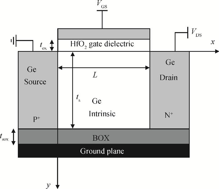
Fig. 1.
Schematic diagram of a Ge TFET.
SEMICONDUCTOR DEVICES
T. S. Arun Samuel and N. B. Balamurugan
Corresponding author: T. S. Arun Samuel, Email:arunsamuel@tce.edu
Abstract: This paper proposes a new two dimensional (2D) analytical model for a germanium (Ge) single gate silicon-on-insulator tunnel field effect transistor (SG SOI TFET). The parabolic approximation technique is used to solve the 2D Poisson equation with suitable boundary conditions and analytical expressions are derived for the surface potential, the electric field along the channel and the vertical electric field. The device output tunnelling current is derived further by using the electric fields. The results show that Ge based TFETs have significant improvements in on-current characteristics. The effectiveness of the proposed model has been verified by comparing the analytical model results with the technology computer aided design (TCAD) simulation results and also comparing them with results from a silicon based TFET.
Keywords: tunnel field effect transistor (TFET), analytical modelling, Poisson equation, surface potential, electric field
| [1] |
Zhang Q, Zhao W, Seabaugh A, et al. Low-subthreshold-swing tunnel transistors. IEEE Electron Device Lett, 2006, 27(4):297 doi: 10.1109/LED.2006.871855
|
| [2] |
Appenzeller J, Lin Y M, Knoch J, et al. Band-to-band tunneling in carbon nanotube field-effect transistors. Phys Rev Lett, 2004, 93(19):196 doi: 10.1103/PhysRevLett.93.196805
|
| [3] |
Toh E H, Wang G H, Chan L, et al. Device design and scalability of a double-gate tunnelling field-effect transistor with silicon-germanium source. Jpn J Appl Phys, 2008, 47(4):2593 doi: 10.1143/JJAP.47.2593
|
| [4] |
Kim S H, Kam H, Hu C, et al. Germanium-source tunnel field effect transistors with record high ION/IOFF. IEEE VLSI Symp on VLSI Technology, 2009:178
|
| [5] |
Boucart K, Ionescu A M. Double-gate tunnel FET with high-k gate dielectric. IEEE Trans Electron Devices, 2007, 54(7):1725 doi: 10.1109/TED.2007.899389
|
| [6] |
Toh E H, Wang G H, Samudra G, et al. Device physics and design of double-gate tunneling field-effect transistor by silicon film thickness optimization. Appl Phys Lett, 2007, 90(26):263 doi: 10.1063/1.2748366?journalCode=apl
|
| [7] |
Damrongplasit N, Shin C. Study of random dopant fluctuation effects in germanium-source tunnel FETs. IEEE Trans Electron Devices, 2011, 58(10):3541 doi: 10.1109/TED.2011.2161990
|
| [8] |
Nayfeh O M, Hoyt J L, Antoniads D A. Strained Si1-xGex/Si band-to-band tunneling transistors:impact of tunnel-junction germanium composition and doping concentration on switching behaviour. IEEE Trans Electron Devices, 2009, 56(10):2264 doi: 10.1109/TED.2009.2028055
|
| [9] |
Toh E H, Wang G H, Samudra G, et al. Device physics and design of germanium tunnelling field-effect transistor with source and drain engineering for low power and high performance applications. J Appl Phys, 2008, 103(10):104504 doi: 10.1063/1.2924413
|
| [10] |
Lee M J. Analytical model of a single-gate silicon-on-insulator (SOI) tunneling field-effect transistors (TFETs). Solid-State Electron, 2011, 63:110 doi: 10.1016/j.sse.2011.05.008
|
| [11] |
Kane. Zener tunneling in semiconductors. J Phys Chem Solids, 1960, 12(2):181 doi: 10.1016/0022-3697(60)90035-4
|
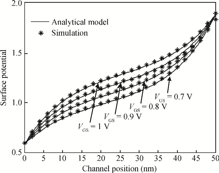
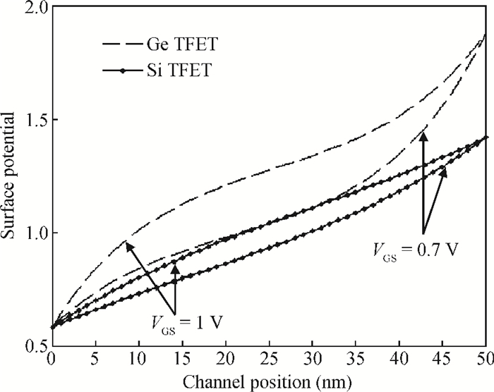
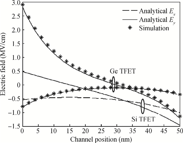
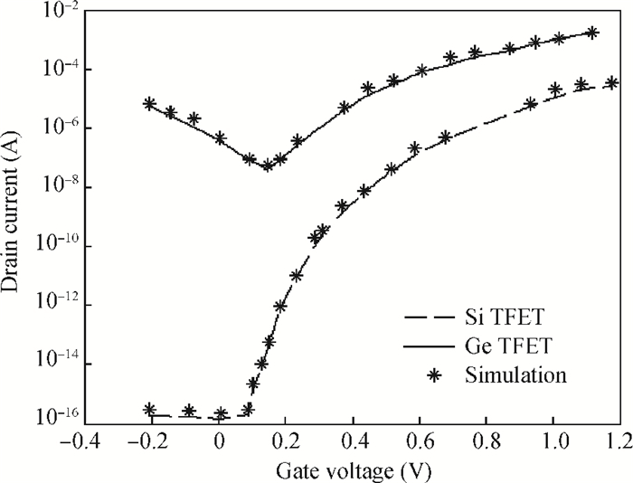
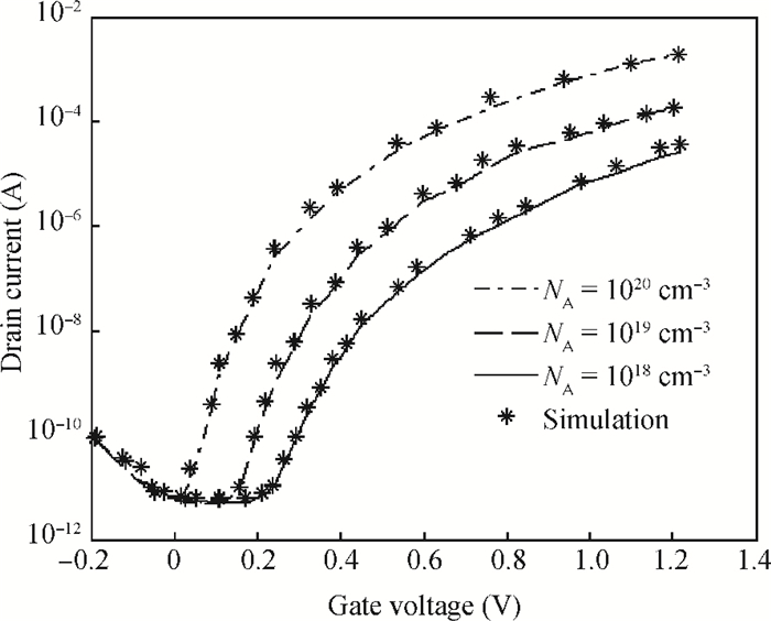
Table 1. Process parameters for simulated Ge TFET.

|
| [1] |
Zhang Q, Zhao W, Seabaugh A, et al. Low-subthreshold-swing tunnel transistors. IEEE Electron Device Lett, 2006, 27(4):297 doi: 10.1109/LED.2006.871855
|
| [2] |
Appenzeller J, Lin Y M, Knoch J, et al. Band-to-band tunneling in carbon nanotube field-effect transistors. Phys Rev Lett, 2004, 93(19):196 doi: 10.1103/PhysRevLett.93.196805
|
| [3] |
Toh E H, Wang G H, Chan L, et al. Device design and scalability of a double-gate tunnelling field-effect transistor with silicon-germanium source. Jpn J Appl Phys, 2008, 47(4):2593 doi: 10.1143/JJAP.47.2593
|
| [4] |
Kim S H, Kam H, Hu C, et al. Germanium-source tunnel field effect transistors with record high ION/IOFF. IEEE VLSI Symp on VLSI Technology, 2009:178
|
| [5] |
Boucart K, Ionescu A M. Double-gate tunnel FET with high-k gate dielectric. IEEE Trans Electron Devices, 2007, 54(7):1725 doi: 10.1109/TED.2007.899389
|
| [6] |
Toh E H, Wang G H, Samudra G, et al. Device physics and design of double-gate tunneling field-effect transistor by silicon film thickness optimization. Appl Phys Lett, 2007, 90(26):263 doi: 10.1063/1.2748366?journalCode=apl
|
| [7] |
Damrongplasit N, Shin C. Study of random dopant fluctuation effects in germanium-source tunnel FETs. IEEE Trans Electron Devices, 2011, 58(10):3541 doi: 10.1109/TED.2011.2161990
|
| [8] |
Nayfeh O M, Hoyt J L, Antoniads D A. Strained Si1-xGex/Si band-to-band tunneling transistors:impact of tunnel-junction germanium composition and doping concentration on switching behaviour. IEEE Trans Electron Devices, 2009, 56(10):2264 doi: 10.1109/TED.2009.2028055
|
| [9] |
Toh E H, Wang G H, Samudra G, et al. Device physics and design of germanium tunnelling field-effect transistor with source and drain engineering for low power and high performance applications. J Appl Phys, 2008, 103(10):104504 doi: 10.1063/1.2924413
|
| [10] |
Lee M J. Analytical model of a single-gate silicon-on-insulator (SOI) tunneling field-effect transistors (TFETs). Solid-State Electron, 2011, 63:110 doi: 10.1016/j.sse.2011.05.008
|
| [11] |
Kane. Zener tunneling in semiconductors. J Phys Chem Solids, 1960, 12(2):181 doi: 10.1016/0022-3697(60)90035-4
|


Article views: 3738 Times PDF downloads: 40 Times Cited by: 0 Times
Received: 02 July 2013 Revised: Online: Published: 01 March 2014
| Citation: |
T. S. Arun Samuel, N. B. Balamurugan. Analytical modeling and simulation of germanium single gate silicon on insulator TFET[J]. Journal of Semiconductors, 2014, 35(3): 034002. doi: 10.1088/1674-4926/35/3/034002
****
T. S. A. Samuel, N. B. Balamurugan. Analytical modeling and simulation of germanium single gate silicon on insulator TFET[J]. J. Semicond., 2014, 35(3): 034002. doi: 10.1088/1674-4926/35/3/034002.

|
| [1] |
Zhang Q, Zhao W, Seabaugh A, et al. Low-subthreshold-swing tunnel transistors. IEEE Electron Device Lett, 2006, 27(4):297 doi: 10.1109/LED.2006.871855
|
| [2] |
Appenzeller J, Lin Y M, Knoch J, et al. Band-to-band tunneling in carbon nanotube field-effect transistors. Phys Rev Lett, 2004, 93(19):196 doi: 10.1103/PhysRevLett.93.196805
|
| [3] |
Toh E H, Wang G H, Chan L, et al. Device design and scalability of a double-gate tunnelling field-effect transistor with silicon-germanium source. Jpn J Appl Phys, 2008, 47(4):2593 doi: 10.1143/JJAP.47.2593
|
| [4] |
Kim S H, Kam H, Hu C, et al. Germanium-source tunnel field effect transistors with record high ION/IOFF. IEEE VLSI Symp on VLSI Technology, 2009:178
|
| [5] |
Boucart K, Ionescu A M. Double-gate tunnel FET with high-k gate dielectric. IEEE Trans Electron Devices, 2007, 54(7):1725 doi: 10.1109/TED.2007.899389
|
| [6] |
Toh E H, Wang G H, Samudra G, et al. Device physics and design of double-gate tunneling field-effect transistor by silicon film thickness optimization. Appl Phys Lett, 2007, 90(26):263 doi: 10.1063/1.2748366?journalCode=apl
|
| [7] |
Damrongplasit N, Shin C. Study of random dopant fluctuation effects in germanium-source tunnel FETs. IEEE Trans Electron Devices, 2011, 58(10):3541 doi: 10.1109/TED.2011.2161990
|
| [8] |
Nayfeh O M, Hoyt J L, Antoniads D A. Strained Si1-xGex/Si band-to-band tunneling transistors:impact of tunnel-junction germanium composition and doping concentration on switching behaviour. IEEE Trans Electron Devices, 2009, 56(10):2264 doi: 10.1109/TED.2009.2028055
|
| [9] |
Toh E H, Wang G H, Samudra G, et al. Device physics and design of germanium tunnelling field-effect transistor with source and drain engineering for low power and high performance applications. J Appl Phys, 2008, 103(10):104504 doi: 10.1063/1.2924413
|
| [10] |
Lee M J. Analytical model of a single-gate silicon-on-insulator (SOI) tunneling field-effect transistors (TFETs). Solid-State Electron, 2011, 63:110 doi: 10.1016/j.sse.2011.05.008
|
| [11] |
Kane. Zener tunneling in semiconductors. J Phys Chem Solids, 1960, 12(2):181 doi: 10.1016/0022-3697(60)90035-4
|

 WeChat ID
Journal of Semiconductors © 2017 All Rights Reserved 京ICP备05085259号-2

 DownLoad:

