


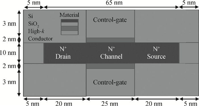
Fig. 1.
Schematic structure of double gate JLFET.
SEMICONDUCTOR DEVICES
Punyasloka Bal1, Bahniman Ghosh1, 2, Partha Mondal1 and M. W. Akram1,
Corresponding author: M. W. Akram, Email:mwakram@iitk.ac.in
Abstract: This paper proposes a laterally graded junctionless transistor taking peak doping concentration near the source and drain region, and a gradual decrease in doping concentration towards the center of the channel to improve the IOFF and ION/IOFF ratio. The decrease of doping concentration in the lateral direction of the channel region depletes a greater number of charge carriers compared to the uniformly doped channel in the OFF-state, which in turn suppresses the OFF state current flowing through the device without greatly affecting the ON state current.
Keywords: junctionless field effect transistor, laterally graded, subthreshold slope
| [1] |
Lilienfeld J E. Method and apparatus for controlling electric current. USA Patent, No. 1745175, Oct. 22, 1925
|
| [2] |
Colinge J P, Lee C W, Afzalian A, et al. Nanowire transistors without junctions. Nat Nanotechnol, 2010, 5(3):225 doi: 10.1038/nnano.2010.15
|
| [3] |
Lee C W, Afzalian A, Akhavan N D, et al. Junctionless multigate field-effect transistor. Appl Phys Lett, 2009, 94(5):053511 doi: 10.1063/1.3079411
|
| [4] |
Lee C W, Ferain I, Kranti A, et al. Short-channel junctionless nanowire transistors. Proc SSDM, 2010:1044 https://confit.atlas.jp/guide/organizer/ssdm/ssdm2010/subject/C-9-5L/search;jsessionid=80FE6AFBC1182DB5EF96DB6241AD7880?eventCode=ssdm2010&code=C-9-5L
|
| [5] |
Kranti A, Yan R, Lee C W, et al. Junctionless nanowire transistor (JNT):properties and design guidelines. Proceedings of the European Solid-State Device Research Conference (ESSDERC), 2010:357 http://www.sciencedirect.com/science/article/pii/S0038110111002139?via%3Dihub
|
| [6] |
Su C J, Tsai T I, Liou Y L, et al. Gate-all-around junctionless transistors with heavily doped polysilicon nanowire channels. IEEE Electron Device Lett, 2011, 32(4):521 doi: 10.1109/LED.2011.2107498
|
| [7] |
Gundapaneni S, Bajaj M, Pandey R K, et al. Effect of band-to-band tunneling on junctionless transistors. IEEE Electron Device Lett, 2012, 59(4):1023 doi: 10.1109/TED.2012.2185800
|
| [8] |
Choi S J, Moon D I, Kim S, et al. Nonvolatile memory by all-around-gate junctionless transistor composed of silicon nanowire on bulk substrate. IEEE Electron Device Lett, 2011, 32(5):602 doi: 10.1109/LED.2011.2118734
|
| [9] |
Lee C W, Yan R, Ferain I, et al. Nanowire zero-capacitor DRAM transistors with and without junctions. Proc 10th IEEE-NANO, 2010:242 http://ieeexplore.ieee.org/abstract/document/5697888/
|
| [10] |
Kranti A, Lee C, Ferain I, et al. Junctionless 6T SRAM cell. IET Electron Lett, 2010, 46(22):1491 doi: 10.1049/el.2010.2736
|
| [11] |
Sels D, Sore B, Groeseneken G. Quantum ballistic transport in the junctionless nanowire pinch-off field effect transistor. J Comput Electron, 2011, 10(1/2):216 http://www.refdoc.fr/Detailnotice?cpsidt=24145533
|
| [12] |
Silvaco, Version 5. 15. 32. R. (2009)[Online]. Available: http://www.silvaco.com
|
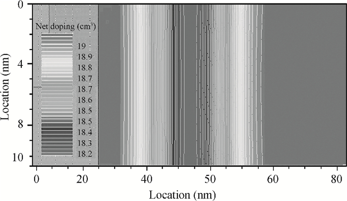
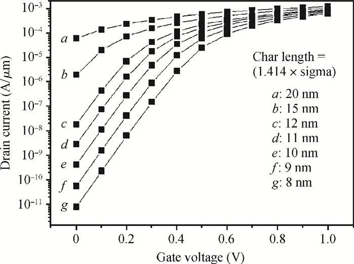
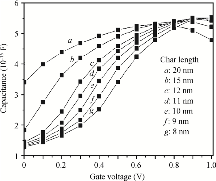
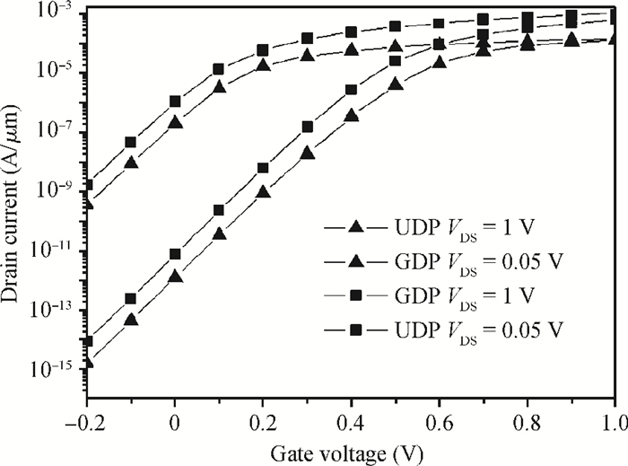
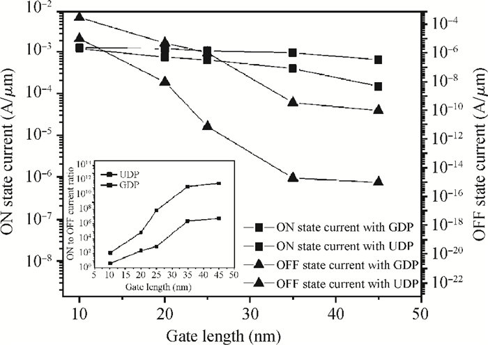
Table 1. Parameters for device simulation.

|
| [1] |
Lilienfeld J E. Method and apparatus for controlling electric current. USA Patent, No. 1745175, Oct. 22, 1925
|
| [2] |
Colinge J P, Lee C W, Afzalian A, et al. Nanowire transistors without junctions. Nat Nanotechnol, 2010, 5(3):225 doi: 10.1038/nnano.2010.15
|
| [3] |
Lee C W, Afzalian A, Akhavan N D, et al. Junctionless multigate field-effect transistor. Appl Phys Lett, 2009, 94(5):053511 doi: 10.1063/1.3079411
|
| [4] |
Lee C W, Ferain I, Kranti A, et al. Short-channel junctionless nanowire transistors. Proc SSDM, 2010:1044 https://confit.atlas.jp/guide/organizer/ssdm/ssdm2010/subject/C-9-5L/search;jsessionid=80FE6AFBC1182DB5EF96DB6241AD7880?eventCode=ssdm2010&code=C-9-5L
|
| [5] |
Kranti A, Yan R, Lee C W, et al. Junctionless nanowire transistor (JNT):properties and design guidelines. Proceedings of the European Solid-State Device Research Conference (ESSDERC), 2010:357 http://www.sciencedirect.com/science/article/pii/S0038110111002139?via%3Dihub
|
| [6] |
Su C J, Tsai T I, Liou Y L, et al. Gate-all-around junctionless transistors with heavily doped polysilicon nanowire channels. IEEE Electron Device Lett, 2011, 32(4):521 doi: 10.1109/LED.2011.2107498
|
| [7] |
Gundapaneni S, Bajaj M, Pandey R K, et al. Effect of band-to-band tunneling on junctionless transistors. IEEE Electron Device Lett, 2012, 59(4):1023 doi: 10.1109/TED.2012.2185800
|
| [8] |
Choi S J, Moon D I, Kim S, et al. Nonvolatile memory by all-around-gate junctionless transistor composed of silicon nanowire on bulk substrate. IEEE Electron Device Lett, 2011, 32(5):602 doi: 10.1109/LED.2011.2118734
|
| [9] |
Lee C W, Yan R, Ferain I, et al. Nanowire zero-capacitor DRAM transistors with and without junctions. Proc 10th IEEE-NANO, 2010:242 http://ieeexplore.ieee.org/abstract/document/5697888/
|
| [10] |
Kranti A, Lee C, Ferain I, et al. Junctionless 6T SRAM cell. IET Electron Lett, 2010, 46(22):1491 doi: 10.1049/el.2010.2736
|
| [11] |
Sels D, Sore B, Groeseneken G. Quantum ballistic transport in the junctionless nanowire pinch-off field effect transistor. J Comput Electron, 2011, 10(1/2):216 http://www.refdoc.fr/Detailnotice?cpsidt=24145533
|
| [12] |
Silvaco, Version 5. 15. 32. R. (2009)[Online]. Available: http://www.silvaco.com
|


Article views: 3325 Times PDF downloads: 20 Times Cited by: 0 Times
Received: 19 July 2013 Revised: Online: Published: 01 March 2014
| Citation: |
Punyasloka Bal, Bahniman Ghosh, Partha Mondal, M. W. Akram. A laterally graded junctionless transistor[J]. Journal of Semiconductors, 2014, 35(3): 034003. doi: 10.1088/1674-4926/35/3/034003
****
P Bal, B Ghosh, P Mondal, M. W. Akram. A laterally graded junctionless transistor[J]. J. Semicond., 2014, 35(3): 034003. doi: 10.1088/1674-4926/35/3/034003.

|
| [1] |
Lilienfeld J E. Method and apparatus for controlling electric current. USA Patent, No. 1745175, Oct. 22, 1925
|
| [2] |
Colinge J P, Lee C W, Afzalian A, et al. Nanowire transistors without junctions. Nat Nanotechnol, 2010, 5(3):225 doi: 10.1038/nnano.2010.15
|
| [3] |
Lee C W, Afzalian A, Akhavan N D, et al. Junctionless multigate field-effect transistor. Appl Phys Lett, 2009, 94(5):053511 doi: 10.1063/1.3079411
|
| [4] |
Lee C W, Ferain I, Kranti A, et al. Short-channel junctionless nanowire transistors. Proc SSDM, 2010:1044 https://confit.atlas.jp/guide/organizer/ssdm/ssdm2010/subject/C-9-5L/search;jsessionid=80FE6AFBC1182DB5EF96DB6241AD7880?eventCode=ssdm2010&code=C-9-5L
|
| [5] |
Kranti A, Yan R, Lee C W, et al. Junctionless nanowire transistor (JNT):properties and design guidelines. Proceedings of the European Solid-State Device Research Conference (ESSDERC), 2010:357 http://www.sciencedirect.com/science/article/pii/S0038110111002139?via%3Dihub
|
| [6] |
Su C J, Tsai T I, Liou Y L, et al. Gate-all-around junctionless transistors with heavily doped polysilicon nanowire channels. IEEE Electron Device Lett, 2011, 32(4):521 doi: 10.1109/LED.2011.2107498
|
| [7] |
Gundapaneni S, Bajaj M, Pandey R K, et al. Effect of band-to-band tunneling on junctionless transistors. IEEE Electron Device Lett, 2012, 59(4):1023 doi: 10.1109/TED.2012.2185800
|
| [8] |
Choi S J, Moon D I, Kim S, et al. Nonvolatile memory by all-around-gate junctionless transistor composed of silicon nanowire on bulk substrate. IEEE Electron Device Lett, 2011, 32(5):602 doi: 10.1109/LED.2011.2118734
|
| [9] |
Lee C W, Yan R, Ferain I, et al. Nanowire zero-capacitor DRAM transistors with and without junctions. Proc 10th IEEE-NANO, 2010:242 http://ieeexplore.ieee.org/abstract/document/5697888/
|
| [10] |
Kranti A, Lee C, Ferain I, et al. Junctionless 6T SRAM cell. IET Electron Lett, 2010, 46(22):1491 doi: 10.1049/el.2010.2736
|
| [11] |
Sels D, Sore B, Groeseneken G. Quantum ballistic transport in the junctionless nanowire pinch-off field effect transistor. J Comput Electron, 2011, 10(1/2):216 http://www.refdoc.fr/Detailnotice?cpsidt=24145533
|
| [12] |
Silvaco, Version 5. 15. 32. R. (2009)[Online]. Available: http://www.silvaco.com
|

 WeChat ID
Journal of Semiconductors © 2017 All Rights Reserved 京ICP备05085259号-2

 DownLoad:

