


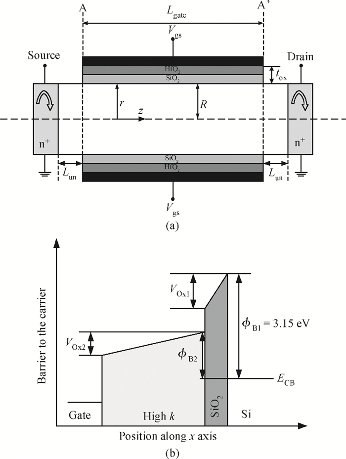
Fig. 1.
(a) Schematic representation of the long-channel cylindrical surrounding-gate MOSFETs structure with gate stack. (b) Potential profile analyzed.
SEMICONDUCTOR DEVICES
Lina Shi, Yiqi Zhuang, Cong Li and Dechang Li
Corresponding author: Shi Lina, Email:shilinaa85819021@163.com
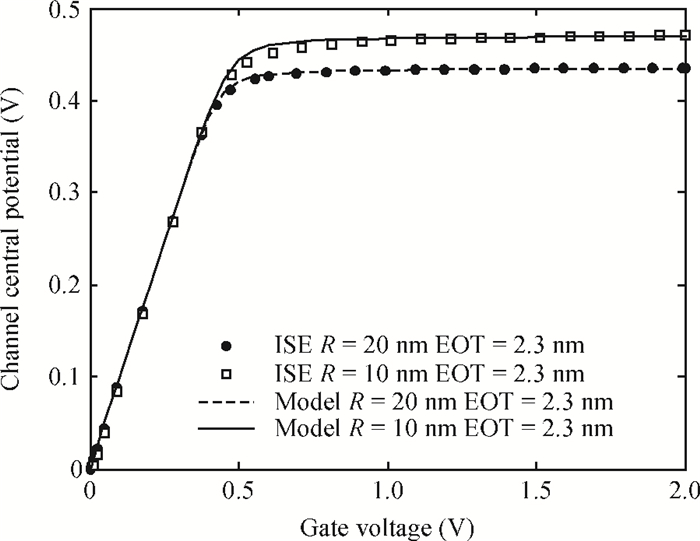
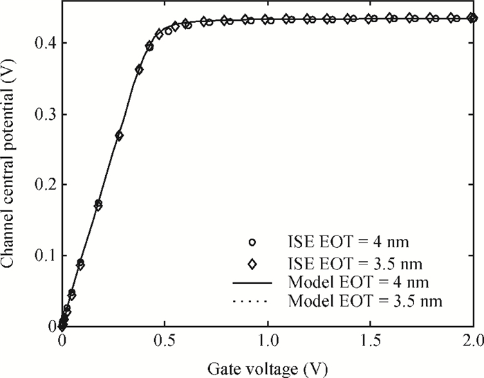
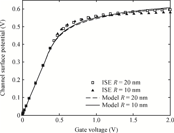
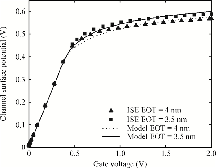
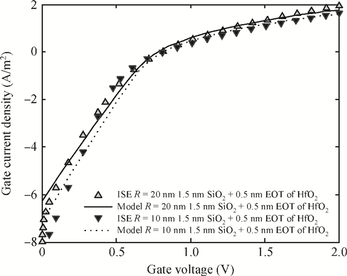
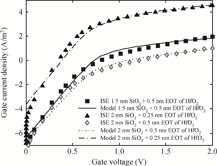
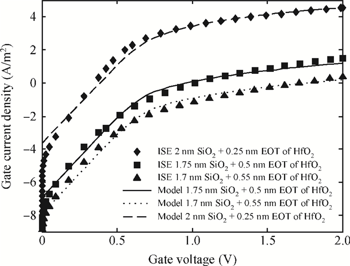
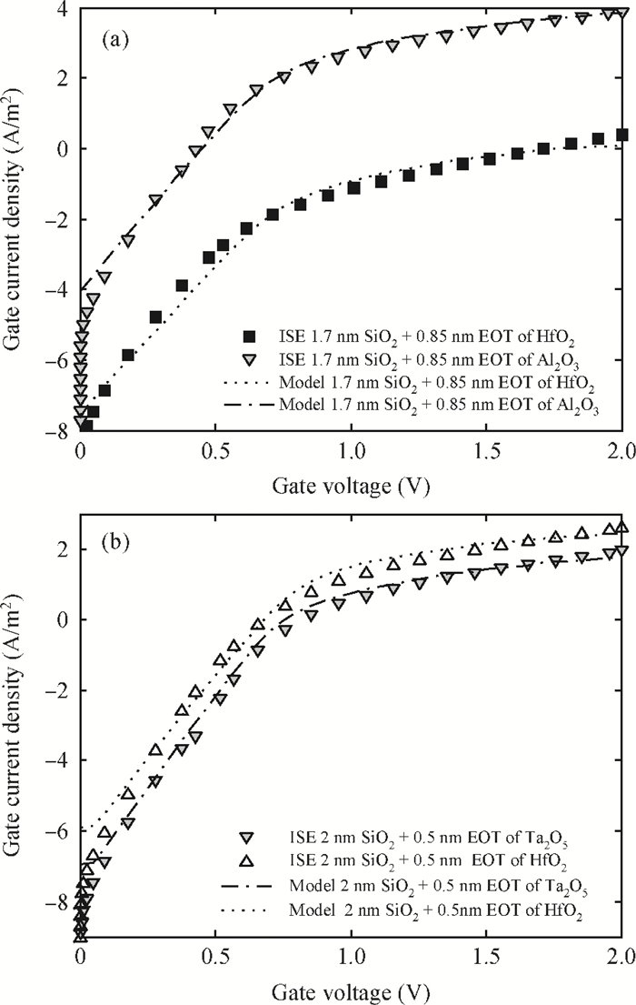
Abstract: An analytical direct tunneling gate current model for cylindrical surrounding gate (CSG) MOSFETs with high-k gate stacks is developed. It is found that the direct tunneling gate current is a strong function of the gate's oxide thickness, but that it is less affected by the change in channel radius. It is also revealed that when the thickness of the equivalent oxide is constant, the thinner the first layer, the smaller the direct tunneling gate current. Moreover, it can be seen that the dielectric with a higher dielectric constant shows a lower tunneling current than expected. The accuracy of the analytical model is verified by the good agreement of its results with those obtained by the three-dimensional numerical device simulator ISE.
Keywords: direct tunneling, gate current, high dielectric, gate stacks, cylindrical surrounding gate MOSFETs
| [1] |
Han R, Li C. Analytical model for direct tunneling gate current in long-channel undoped cylindrical surrounding gate metal-oxide-semiconductor field effect transistors. Jpn J Appl Phys, 2013, 52(2):024302 doi: 10.7567/JJAP.52.024302/meta;jsessionid=9D75E5C220A9027B9385D280AD3A9214.c3.iopscience.cld.iop.org
|
| [2] |
Li C, Zhuang Y, Han R. Cylindrical surrounding-gate MOSFETs with electrically induced source/drain extension. Microelectron J, 2011, 42(2):341 doi: 10.1016/j.mejo.2010.11.010
|
| [3] |
Ghosh P, Haldar S, Gupta R S, et al. An analytical drain current model for dual material engineered cylindrical/surrounded gate MOSFET. Microelectron J, 2012, 43(1):17 doi: 10.1016/j.mejo.2011.10.001
|
| [4] |
Darbandy G, Ritzenthaler R, Lime F, et al. Analytical modeling of the gate tunneling leakage for the determination of adequate high-k dielectrics in double-gate SOI MOSFETs at the 22 nm node. Solid-State Electron, 2010, 54(10):1083 doi: 10.1016/j.sse.2010.06.015
|
| [5] |
Zhong Xinghua, Wu Junfeng, Yang Jianjun, et al. Electrical properties of ultra thin nitride/oxynitride stack dielectrics pMOS capacitor with refractory metal gate. Chinese Journal of Semiconductors, 2005, 26(4):651 http://www.oalib.com/paper/1519803#.WcSsf_lJLy8
|
| [6] |
Zhao Y, White M H. Modeling of direct tunneling current through interfacial oxide and high-k gate stacks. Solid-State Electron, 2004, 48(10/11):1801 https://www.researchgate.net/publication/243274930_Modeling_of_direct_tunneling_current_through_interfacial_oxide_and_high-_K_gate_stacks
|
| [7] |
Yang N, Henson W K, Hauser J R, et al. Modeling study of ultrathin gate oxides using direct tunneling current and capacitance-voltage measurements in MOS devices. IEEE Trans Electron Devices, 1999, 46(7):1464 doi: 10.1109/16.772492
|
| [8] |
Zheng Changyong, Zhang Wei, Xu Tailong, et al. A compact model for single material double work function gate MOSFET. Journal of Semiconductors, 2013, 34(9):094006 doi: 10.1088/1674-4926/34/9/094006
|
| [9] |
Lee J C, Cho H J, Kang C S, et al. High-k dielectrics and MOSFET characteristics. IEDM Tech Dig, Washington, DC, USA, 2003 http://ieeexplore.ieee.org/document/1269174/
|
| [10] |
Wang W, Gu N, Sun J P, et al. Gate current modeling of high-k stack nanoscale MOSFETs. Solid-State Electron, 2006, 50(9/10):1489 doi: 10.1002/pssc.v6:12
|
| [11] |
Wang W, Gu N, Sun J P, et al. Gate current modeling of high-k stack nanoscale MOSFETs. Solid-State Electron, 2006, 50(9/10):1489 https://experts.umich.edu/en/publications/gate-current-modeling-of-
|
| [12] |
Chaujar R, Kaur R, Saxena M, et al. Investigation of multi-layered-gate electrode workfunction engineered recessed channel (MLGEW E-RC) sub-50 nm MOSFET:a novel design. International Journal of Numerical Modelling:Electronic Networks, Devices and Fields, 2009, 22(3):259 doi: 10.1002/jnm.v22:3
|
| [13] |
Kauerauf T, Govoreanu B, Degraeve R, et al. Finding the gate stack with the lowest leakage current. Solid-State Electron, 2005, 49(5):695 doi: 10.1016/j.sse.2005.01.018
|
| [14] |
Darbandy G, Lime F, Cerdeira A, et al. Study of potential high-k dielectric for UTB SOI MOSFETs using analytical modeling of the gate tunneling leakage. Semicond Sci Technol, 2011, 26(11):115002 doi: 10.1088/0268-1242/26/11/115002
|
| [15] |
Cerdeira A, Moldovan O, Iniguez B, et al. Modeling of potentials and threshold voltage for symmetric doped double-gate MOSFETs. Solid-State Electron, 2008, 52(5):830 doi: 10.1016/j.sse.2007.10.046
|
| [16] |
Cerdeira A, Iniguez B, Estrada M. Compact model for short channel symmetric doped double-gate MOSFETs. Solid-State Electron, 2008, 52(7):1064 doi: 10.1016/j.sse.2008.03.009
|
| [17] |
Li C, Zhuang Y, Han R. Analytical threshold model for nanoscale cylindrical surrounding-gate metal-oxide-semiconductor field effect transistor with high-k gate dielectric and tri-material gate stack. Jpn J Appl Phys, 2010, 49(12):124202 doi: 10.1143/JJAP.49.124202
|
| [18] |
Darbandy G, Ritzenthaler R, Lime F, et al. Analytical modeling of direct tunneling current through gate stacks for the determination of suitable high-k dielectrics for nanoscale double-gate MOSFETs. Semicond Sci Technol, 2011, 26(4):045002 doi: 10.1088/0268-1242/26/4/045002
|
| [19] |
Houssa M, Tuominen M, Naili M, et al. Trap-assisted tunneling in high permittivity gate dielectric stacks. J Appl Phys, 2000, 87(12):8615 doi: 10.1063/1.373587
|
| [20] |
Garduño S I, Cerdeira A, Estrada M. Inclusion of direct tunneling gate current in the symmetric doped double gate MOSFETs model. 6th International Conference on Electrical Engineering, Computing Science and Automation Control, University of Autonoma Estado Mexico, FacIngenieria, Toluca, Mexico, 2009 http://ieeexplore.ieee.org/document/5393382/
|
| [21] |
Lee W C, Hu C. Modeling CMOS tunneling currents through ultrathin gate oxide due to conduction-and valence-band electron and hole tunneling. IEEE Trans Electron Devices, 2001, 48(7):1366 doi: 10.1109/16.930653
|


Article views: 3123 Times PDF downloads: 28 Times Cited by: 0 Times
Received: 19 August 2013 Revised: 18 October 2013 Online: Published: 01 March 2014
| Citation: |
Lina Shi, Yiqi Zhuang, Cong Li, Dechang Li. Analytical modeling of the direct tunneling current through high-k gate stacks for long-channel cylindrical surrounding-gate MOSFETs[J]. Journal of Semiconductors, 2014, 35(3): 034009. doi: 10.1088/1674-4926/35/3/034009
****
L N Shi, Y Q Zhuang, C Li, D C Li. Analytical modeling of the direct tunneling current through high-k gate stacks for long-channel cylindrical surrounding-gate MOSFETs[J]. J. Semicond., 2014, 35(3): 034009. doi: 10.1088/1674-4926/35/3/034009.

|
| [1] |
Han R, Li C. Analytical model for direct tunneling gate current in long-channel undoped cylindrical surrounding gate metal-oxide-semiconductor field effect transistors. Jpn J Appl Phys, 2013, 52(2):024302 doi: 10.7567/JJAP.52.024302/meta;jsessionid=9D75E5C220A9027B9385D280AD3A9214.c3.iopscience.cld.iop.org
|
| [2] |
Li C, Zhuang Y, Han R. Cylindrical surrounding-gate MOSFETs with electrically induced source/drain extension. Microelectron J, 2011, 42(2):341 doi: 10.1016/j.mejo.2010.11.010
|
| [3] |
Ghosh P, Haldar S, Gupta R S, et al. An analytical drain current model for dual material engineered cylindrical/surrounded gate MOSFET. Microelectron J, 2012, 43(1):17 doi: 10.1016/j.mejo.2011.10.001
|
| [4] |
Darbandy G, Ritzenthaler R, Lime F, et al. Analytical modeling of the gate tunneling leakage for the determination of adequate high-k dielectrics in double-gate SOI MOSFETs at the 22 nm node. Solid-State Electron, 2010, 54(10):1083 doi: 10.1016/j.sse.2010.06.015
|
| [5] |
Zhong Xinghua, Wu Junfeng, Yang Jianjun, et al. Electrical properties of ultra thin nitride/oxynitride stack dielectrics pMOS capacitor with refractory metal gate. Chinese Journal of Semiconductors, 2005, 26(4):651 http://www.oalib.com/paper/1519803#.WcSsf_lJLy8
|
| [6] |
Zhao Y, White M H. Modeling of direct tunneling current through interfacial oxide and high-k gate stacks. Solid-State Electron, 2004, 48(10/11):1801 https://www.researchgate.net/publication/243274930_Modeling_of_direct_tunneling_current_through_interfacial_oxide_and_high-_K_gate_stacks
|
| [7] |
Yang N, Henson W K, Hauser J R, et al. Modeling study of ultrathin gate oxides using direct tunneling current and capacitance-voltage measurements in MOS devices. IEEE Trans Electron Devices, 1999, 46(7):1464 doi: 10.1109/16.772492
|
| [8] |
Zheng Changyong, Zhang Wei, Xu Tailong, et al. A compact model for single material double work function gate MOSFET. Journal of Semiconductors, 2013, 34(9):094006 doi: 10.1088/1674-4926/34/9/094006
|
| [9] |
Lee J C, Cho H J, Kang C S, et al. High-k dielectrics and MOSFET characteristics. IEDM Tech Dig, Washington, DC, USA, 2003 http://ieeexplore.ieee.org/document/1269174/
|
| [10] |
Wang W, Gu N, Sun J P, et al. Gate current modeling of high-k stack nanoscale MOSFETs. Solid-State Electron, 2006, 50(9/10):1489 doi: 10.1002/pssc.v6:12
|
| [11] |
Wang W, Gu N, Sun J P, et al. Gate current modeling of high-k stack nanoscale MOSFETs. Solid-State Electron, 2006, 50(9/10):1489 https://experts.umich.edu/en/publications/gate-current-modeling-of-
|
| [12] |
Chaujar R, Kaur R, Saxena M, et al. Investigation of multi-layered-gate electrode workfunction engineered recessed channel (MLGEW E-RC) sub-50 nm MOSFET:a novel design. International Journal of Numerical Modelling:Electronic Networks, Devices and Fields, 2009, 22(3):259 doi: 10.1002/jnm.v22:3
|
| [13] |
Kauerauf T, Govoreanu B, Degraeve R, et al. Finding the gate stack with the lowest leakage current. Solid-State Electron, 2005, 49(5):695 doi: 10.1016/j.sse.2005.01.018
|
| [14] |
Darbandy G, Lime F, Cerdeira A, et al. Study of potential high-k dielectric for UTB SOI MOSFETs using analytical modeling of the gate tunneling leakage. Semicond Sci Technol, 2011, 26(11):115002 doi: 10.1088/0268-1242/26/11/115002
|
| [15] |
Cerdeira A, Moldovan O, Iniguez B, et al. Modeling of potentials and threshold voltage for symmetric doped double-gate MOSFETs. Solid-State Electron, 2008, 52(5):830 doi: 10.1016/j.sse.2007.10.046
|
| [16] |
Cerdeira A, Iniguez B, Estrada M. Compact model for short channel symmetric doped double-gate MOSFETs. Solid-State Electron, 2008, 52(7):1064 doi: 10.1016/j.sse.2008.03.009
|
| [17] |
Li C, Zhuang Y, Han R. Analytical threshold model for nanoscale cylindrical surrounding-gate metal-oxide-semiconductor field effect transistor with high-k gate dielectric and tri-material gate stack. Jpn J Appl Phys, 2010, 49(12):124202 doi: 10.1143/JJAP.49.124202
|
| [18] |
Darbandy G, Ritzenthaler R, Lime F, et al. Analytical modeling of direct tunneling current through gate stacks for the determination of suitable high-k dielectrics for nanoscale double-gate MOSFETs. Semicond Sci Technol, 2011, 26(4):045002 doi: 10.1088/0268-1242/26/4/045002
|
| [19] |
Houssa M, Tuominen M, Naili M, et al. Trap-assisted tunneling in high permittivity gate dielectric stacks. J Appl Phys, 2000, 87(12):8615 doi: 10.1063/1.373587
|
| [20] |
Garduño S I, Cerdeira A, Estrada M. Inclusion of direct tunneling gate current in the symmetric doped double gate MOSFETs model. 6th International Conference on Electrical Engineering, Computing Science and Automation Control, University of Autonoma Estado Mexico, FacIngenieria, Toluca, Mexico, 2009 http://ieeexplore.ieee.org/document/5393382/
|
| [21] |
Lee W C, Hu C. Modeling CMOS tunneling currents through ultrathin gate oxide due to conduction-and valence-band electron and hole tunneling. IEEE Trans Electron Devices, 2001, 48(7):1366 doi: 10.1109/16.930653
|

 WeChat ID
Journal of Semiconductors © 2017 All Rights Reserved 京ICP备05085259号-2

 DownLoad:

