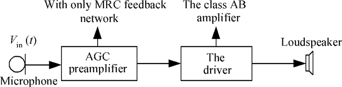
Fig. 1.
The conventional hearing aid system.
SEMICONDUCTOR INTEGRATED CIRCUITS
Fanyang Li and Hao Jiang
Corresponding author: Li Fanyang, Email:qingsheng11081@sina.com
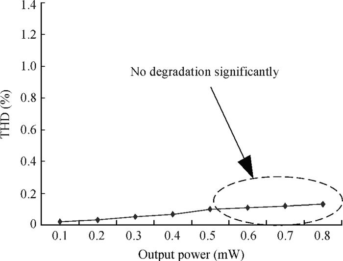
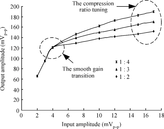
Abstract: A hearing aid on-chip system based on accuracy optimized front-and back-end blocks is presented for enhancing the signal processing accuracy of the hearing aid. Compared with the conventional system, the accuracy optimized system is characterized by the dual feedback network and the gain compensation technique used in the front-and back-end blocks, respectively, so as to alleviate the nonlinearity distortion caused by the output swing. By using the technique, the accuracy of the whole hearing aid system can be significantly improved. The prototype chip has been designed with a 0.13 μm standard CMOS process and tested with 1 V supply voltage. The measurement results show that, for driving a 16 Ω loudspeaker with a normalized output level of 300 mVp-p, the total harmonic distortion reached about -60 dB, achieving at least three times reduction compared to the previously reported works. In addition, the typical input referred noise is only about 5 μ Vrms.
Keywords: front-end, back-end, pre-amplifier, driving amplifier, hearing aid
| [1] |
Gata D G, Sjursen W, Hochschild J R, et al. A 1.1 V 270μ A mixed-signal hearing aid chip. IEEE J Solid-State Circuits, 2002, 37(12):1670 doi: 10.1109/JSSC.2002.804328
|
| [2] |
Silva-Martinez J, Solis-Bustos S, Schellenberg M. A CMOS hearing aid device. Analog Integrated Circuit and Signal Processing, 1999, SC-21(2):163 http://dl.acm.org/citation.cfm?id=339109
|
| [3] |
Serra-Graells F, Gomez L, Huertas J L. A true-l-V 300-μ W CMOS-sub threshold log-domain hearing-aid-on-chip. IEEE J Solid-State Circuits, 2004, 39(8):1271 doi: 10.1109/JSSC.2004.831469
|
| [4] |
Serra-Graells F, Huertas J L. Low voltage CMOS-sub threshold log amplification and AGC. IEE Proc Circuits Devices Syst, 2005, 152(1):61 doi: 10.1049/ip-cds:20041003
|
| [5] |
Azzolini C, Boni A. A 1-V CMOS audio amplifier for low cost hearing aids. Proc 15th IEEE Int Conf on Electronics, Circuit and Systems, St. Julien's, 2008:562 http://ieeexplore.ieee.org/xpl/abstractKeywords.jsp?reload=true&arnumber=4674915
|
| [6] |
Hauptmann J, Dielacher F, Steiner R. A low-noise amplifier with automatic gain control and anti-clipping control in CMOS technology. IEEE J Solid-State Circuits, 1992, SC-27(7):974 http://ieeexplore.ieee.org/xpls/abs_all.jsp?arnumber=142591
|
| [7] |
Kim S, Lee J Y, Song S J, et al. An energy-efficient analog front-end circuit for a sub-1 V digital hearing aid. IEEE J Solid-State Circuits, 2006, SC-41(4):876 http://ieeexplore.ieee.org/document/1610632/
|
| [8] |
Li F, Yang H, Liu F, et al. Dual-mode gain control for a 1 V CMOS hearing aid device with enhanced accuracy and energy-efficiency. Journal of Analog Integrated Circuit and Signal Processing, 2012, 72(2):495 doi: 10.1007/s10470-012-9844-5
|
| [9] |
IEC. Hearing aids with automatic gain control circuits. Technical Report 118-2, 1983 http://infostore.saiglobal.com/store/Details.aspx?productID=661208
|
| [10] |
Zhak S M, Baker M W. A low-power wide dynamic range envelop detector. IEEE J Solid-State Circuits, 2003, SC-38(10):1750 http://ieeexplore.ieee.org/xpls/icp.jsp?arnumber=1233793
|
| [11] |
Sarpeshkar R, Baker M W, Salthouse C D, et al. An analog bionic ear processor with zero-crossing detection. Proc ISSCC, San Francisco, CA, 2005:78 http://ieeexplore.ieee.org/xpl/articleDetails.jsp?arnumber=1493877&filter%3DAND%28p_IS_Number%3A32118%29
|
| [12] |
Panagiotopulos D A, Newcomb R W, Singh S K. A current-mode exponential amplifier. IEEE Trans Circuit Syst Ⅱ, Analog Digit Signal Process, 2000, SC-47(6):548 http://ieeexplore.ieee.org/stamp/stamp.jsp?tp=&isnumber=18384&arnumber=847071
|
| [13] |
Zou X, Lian Y. A 1-V 450 nW fully integrated programmable biomedical sensor interface chip. IEEE J Solid-State Circuits, 2009, SC-44(4):1067 http://ieeexplore.ieee.org/xpl/freeabs_all.jsp?arnumber=4805128
|
| [14] |
Serra-Graells F. VLSI CMOS low-voltage log companding filters. Proc IEEE Int Symp on Circuit and Systems, 2000, 1:172 http://ieeexplore.ieee.org/xpl/articleDetails.jsp?reload=true&arnumber=857055&contentType=Conference+Publications
|
| [15] |
Floru F. Attack and release time constants in RMS-based feedback compressors. J Audio Eng Soc, 1999, 47(10):788 http://www.aes.org/e-lib/download.cfm?ID=12090
|
| [16] |
Pickles J O. Introduction to the physiology of hearing. 2nd ed. New York:Academic Press, 1988
|
| [17] |
Kim M G, Ahn G C, Hanumolu P K. A 0.9 V 92 dB double-sampled switched-RC delta-sigma audio ADC. IEEE J Solid-State Circuit, 2008, SC-43(5):1195 http://ieeexplore.ieee.org/xpl/articleDetails.jsp?arnumber=4494661&contentType=Journals+%26+Magazines
|
| [18] |
Sarpeshar R, Delbruck T, Mead C. White noise in MOS transistors and resistors. IEEE Circuit Devices Mag, 1993, 9(6):23 doi: 10.1109/101.261888
|
| [19] |
The product of hearing aid chip. The Corp of Genum, 2001
|
| [20] |
Deligoz I, Naqvi S R. A MEMS-based power-scalable hearing aid analog front end. IEEE Trans Biomedical Circuit Syst, 2011, 5(3):201 doi: 10.1109/TBCAS.2010.2079329
|
| [21] |
Farouk T, Mohieldin A N, Khalil A H. Low-voltage low-power CMOS fully differential linear transconductor with mobility reduction compensation. Microelectron J, 2012, 43(1):69 doi: 10.1016/j.mejo.2011.11.001
|
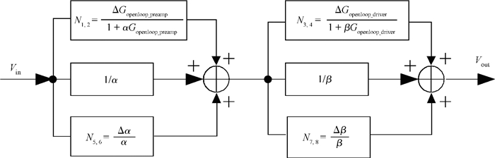
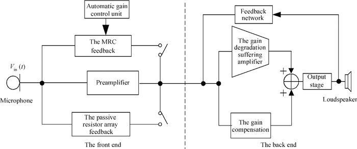
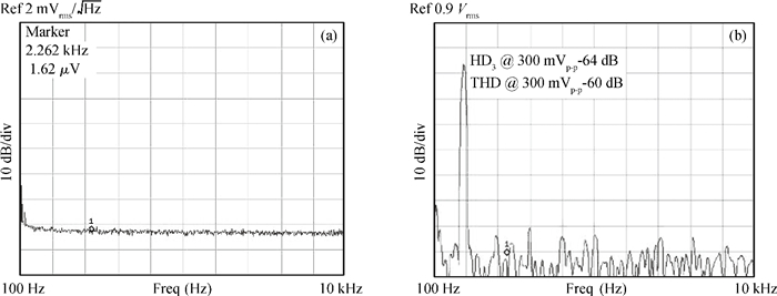
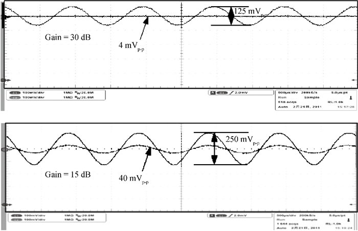
Table 1. Performance comparison.

|
| [1] |
Gata D G, Sjursen W, Hochschild J R, et al. A 1.1 V 270μ A mixed-signal hearing aid chip. IEEE J Solid-State Circuits, 2002, 37(12):1670 doi: 10.1109/JSSC.2002.804328
|
| [2] |
Silva-Martinez J, Solis-Bustos S, Schellenberg M. A CMOS hearing aid device. Analog Integrated Circuit and Signal Processing, 1999, SC-21(2):163 http://dl.acm.org/citation.cfm?id=339109
|
| [3] |
Serra-Graells F, Gomez L, Huertas J L. A true-l-V 300-μ W CMOS-sub threshold log-domain hearing-aid-on-chip. IEEE J Solid-State Circuits, 2004, 39(8):1271 doi: 10.1109/JSSC.2004.831469
|
| [4] |
Serra-Graells F, Huertas J L. Low voltage CMOS-sub threshold log amplification and AGC. IEE Proc Circuits Devices Syst, 2005, 152(1):61 doi: 10.1049/ip-cds:20041003
|
| [5] |
Azzolini C, Boni A. A 1-V CMOS audio amplifier for low cost hearing aids. Proc 15th IEEE Int Conf on Electronics, Circuit and Systems, St. Julien's, 2008:562 http://ieeexplore.ieee.org/xpl/abstractKeywords.jsp?reload=true&arnumber=4674915
|
| [6] |
Hauptmann J, Dielacher F, Steiner R. A low-noise amplifier with automatic gain control and anti-clipping control in CMOS technology. IEEE J Solid-State Circuits, 1992, SC-27(7):974 http://ieeexplore.ieee.org/xpls/abs_all.jsp?arnumber=142591
|
| [7] |
Kim S, Lee J Y, Song S J, et al. An energy-efficient analog front-end circuit for a sub-1 V digital hearing aid. IEEE J Solid-State Circuits, 2006, SC-41(4):876 http://ieeexplore.ieee.org/document/1610632/
|
| [8] |
Li F, Yang H, Liu F, et al. Dual-mode gain control for a 1 V CMOS hearing aid device with enhanced accuracy and energy-efficiency. Journal of Analog Integrated Circuit and Signal Processing, 2012, 72(2):495 doi: 10.1007/s10470-012-9844-5
|
| [9] |
IEC. Hearing aids with automatic gain control circuits. Technical Report 118-2, 1983 http://infostore.saiglobal.com/store/Details.aspx?productID=661208
|
| [10] |
Zhak S M, Baker M W. A low-power wide dynamic range envelop detector. IEEE J Solid-State Circuits, 2003, SC-38(10):1750 http://ieeexplore.ieee.org/xpls/icp.jsp?arnumber=1233793
|
| [11] |
Sarpeshkar R, Baker M W, Salthouse C D, et al. An analog bionic ear processor with zero-crossing detection. Proc ISSCC, San Francisco, CA, 2005:78 http://ieeexplore.ieee.org/xpl/articleDetails.jsp?arnumber=1493877&filter%3DAND%28p_IS_Number%3A32118%29
|
| [12] |
Panagiotopulos D A, Newcomb R W, Singh S K. A current-mode exponential amplifier. IEEE Trans Circuit Syst Ⅱ, Analog Digit Signal Process, 2000, SC-47(6):548 http://ieeexplore.ieee.org/stamp/stamp.jsp?tp=&isnumber=18384&arnumber=847071
|
| [13] |
Zou X, Lian Y. A 1-V 450 nW fully integrated programmable biomedical sensor interface chip. IEEE J Solid-State Circuits, 2009, SC-44(4):1067 http://ieeexplore.ieee.org/xpl/freeabs_all.jsp?arnumber=4805128
|
| [14] |
Serra-Graells F. VLSI CMOS low-voltage log companding filters. Proc IEEE Int Symp on Circuit and Systems, 2000, 1:172 http://ieeexplore.ieee.org/xpl/articleDetails.jsp?reload=true&arnumber=857055&contentType=Conference+Publications
|
| [15] |
Floru F. Attack and release time constants in RMS-based feedback compressors. J Audio Eng Soc, 1999, 47(10):788 http://www.aes.org/e-lib/download.cfm?ID=12090
|
| [16] |
Pickles J O. Introduction to the physiology of hearing. 2nd ed. New York:Academic Press, 1988
|
| [17] |
Kim M G, Ahn G C, Hanumolu P K. A 0.9 V 92 dB double-sampled switched-RC delta-sigma audio ADC. IEEE J Solid-State Circuit, 2008, SC-43(5):1195 http://ieeexplore.ieee.org/xpl/articleDetails.jsp?arnumber=4494661&contentType=Journals+%26+Magazines
|
| [18] |
Sarpeshar R, Delbruck T, Mead C. White noise in MOS transistors and resistors. IEEE Circuit Devices Mag, 1993, 9(6):23 doi: 10.1109/101.261888
|
| [19] |
The product of hearing aid chip. The Corp of Genum, 2001
|
| [20] |
Deligoz I, Naqvi S R. A MEMS-based power-scalable hearing aid analog front end. IEEE Trans Biomedical Circuit Syst, 2011, 5(3):201 doi: 10.1109/TBCAS.2010.2079329
|
| [21] |
Farouk T, Mohieldin A N, Khalil A H. Low-voltage low-power CMOS fully differential linear transconductor with mobility reduction compensation. Microelectron J, 2012, 43(1):69 doi: 10.1016/j.mejo.2011.11.001
|


Article views: 2551 Times PDF downloads: 14 Times Cited by: 0 Times
Received: 28 August 2013 Revised: 29 September 2013 Online: Published: 01 March 2014
| Citation: |
Fanyang Li, Hao Jiang. A hearing aid on-chip system based on accuracy optimized front-and back-end blocks[J]. Journal of Semiconductors, 2014, 35(3): 035006. doi: 10.1088/1674-4926/35/3/035006
****
F Y Li, H Jiang. A hearing aid on-chip system based on accuracy optimized front-and back-end blocks[J]. J. Semicond., 2014, 35(3): 035006. doi: 10.1088/1674-4926/35/3/035006.

|
| [1] |
Gata D G, Sjursen W, Hochschild J R, et al. A 1.1 V 270μ A mixed-signal hearing aid chip. IEEE J Solid-State Circuits, 2002, 37(12):1670 doi: 10.1109/JSSC.2002.804328
|
| [2] |
Silva-Martinez J, Solis-Bustos S, Schellenberg M. A CMOS hearing aid device. Analog Integrated Circuit and Signal Processing, 1999, SC-21(2):163 http://dl.acm.org/citation.cfm?id=339109
|
| [3] |
Serra-Graells F, Gomez L, Huertas J L. A true-l-V 300-μ W CMOS-sub threshold log-domain hearing-aid-on-chip. IEEE J Solid-State Circuits, 2004, 39(8):1271 doi: 10.1109/JSSC.2004.831469
|
| [4] |
Serra-Graells F, Huertas J L. Low voltage CMOS-sub threshold log amplification and AGC. IEE Proc Circuits Devices Syst, 2005, 152(1):61 doi: 10.1049/ip-cds:20041003
|
| [5] |
Azzolini C, Boni A. A 1-V CMOS audio amplifier for low cost hearing aids. Proc 15th IEEE Int Conf on Electronics, Circuit and Systems, St. Julien's, 2008:562 http://ieeexplore.ieee.org/xpl/abstractKeywords.jsp?reload=true&arnumber=4674915
|
| [6] |
Hauptmann J, Dielacher F, Steiner R. A low-noise amplifier with automatic gain control and anti-clipping control in CMOS technology. IEEE J Solid-State Circuits, 1992, SC-27(7):974 http://ieeexplore.ieee.org/xpls/abs_all.jsp?arnumber=142591
|
| [7] |
Kim S, Lee J Y, Song S J, et al. An energy-efficient analog front-end circuit for a sub-1 V digital hearing aid. IEEE J Solid-State Circuits, 2006, SC-41(4):876 http://ieeexplore.ieee.org/document/1610632/
|
| [8] |
Li F, Yang H, Liu F, et al. Dual-mode gain control for a 1 V CMOS hearing aid device with enhanced accuracy and energy-efficiency. Journal of Analog Integrated Circuit and Signal Processing, 2012, 72(2):495 doi: 10.1007/s10470-012-9844-5
|
| [9] |
IEC. Hearing aids with automatic gain control circuits. Technical Report 118-2, 1983 http://infostore.saiglobal.com/store/Details.aspx?productID=661208
|
| [10] |
Zhak S M, Baker M W. A low-power wide dynamic range envelop detector. IEEE J Solid-State Circuits, 2003, SC-38(10):1750 http://ieeexplore.ieee.org/xpls/icp.jsp?arnumber=1233793
|
| [11] |
Sarpeshkar R, Baker M W, Salthouse C D, et al. An analog bionic ear processor with zero-crossing detection. Proc ISSCC, San Francisco, CA, 2005:78 http://ieeexplore.ieee.org/xpl/articleDetails.jsp?arnumber=1493877&filter%3DAND%28p_IS_Number%3A32118%29
|
| [12] |
Panagiotopulos D A, Newcomb R W, Singh S K. A current-mode exponential amplifier. IEEE Trans Circuit Syst Ⅱ, Analog Digit Signal Process, 2000, SC-47(6):548 http://ieeexplore.ieee.org/stamp/stamp.jsp?tp=&isnumber=18384&arnumber=847071
|
| [13] |
Zou X, Lian Y. A 1-V 450 nW fully integrated programmable biomedical sensor interface chip. IEEE J Solid-State Circuits, 2009, SC-44(4):1067 http://ieeexplore.ieee.org/xpl/freeabs_all.jsp?arnumber=4805128
|
| [14] |
Serra-Graells F. VLSI CMOS low-voltage log companding filters. Proc IEEE Int Symp on Circuit and Systems, 2000, 1:172 http://ieeexplore.ieee.org/xpl/articleDetails.jsp?reload=true&arnumber=857055&contentType=Conference+Publications
|
| [15] |
Floru F. Attack and release time constants in RMS-based feedback compressors. J Audio Eng Soc, 1999, 47(10):788 http://www.aes.org/e-lib/download.cfm?ID=12090
|
| [16] |
Pickles J O. Introduction to the physiology of hearing. 2nd ed. New York:Academic Press, 1988
|
| [17] |
Kim M G, Ahn G C, Hanumolu P K. A 0.9 V 92 dB double-sampled switched-RC delta-sigma audio ADC. IEEE J Solid-State Circuit, 2008, SC-43(5):1195 http://ieeexplore.ieee.org/xpl/articleDetails.jsp?arnumber=4494661&contentType=Journals+%26+Magazines
|
| [18] |
Sarpeshar R, Delbruck T, Mead C. White noise in MOS transistors and resistors. IEEE Circuit Devices Mag, 1993, 9(6):23 doi: 10.1109/101.261888
|
| [19] |
The product of hearing aid chip. The Corp of Genum, 2001
|
| [20] |
Deligoz I, Naqvi S R. A MEMS-based power-scalable hearing aid analog front end. IEEE Trans Biomedical Circuit Syst, 2011, 5(3):201 doi: 10.1109/TBCAS.2010.2079329
|
| [21] |
Farouk T, Mohieldin A N, Khalil A H. Low-voltage low-power CMOS fully differential linear transconductor with mobility reduction compensation. Microelectron J, 2012, 43(1):69 doi: 10.1016/j.mejo.2011.11.001
|

 WeChat ID
Journal of Semiconductors © 2017 All Rights Reserved 京ICP备05085259号-2

 DownLoad: