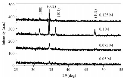
Fig. 1.
X-ray diffraction spectra of ZnO thin films as a function of spray concentration.
SEMICONDUCTOR PHYSICS
S. Benramache1, , O. Belahssen1, 2, 3, A. Guettaf4 and A. Arif4
Corresponding author: S. Benramache, Email: saidzno2006@gmail.com
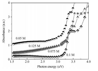
Abstract: We investigated the structural and optical properties of ZnO thin films as an n-type semiconductor. The films were deposited at different precursor molarities using an ultrasonic spray method. In this paper we focused our attention on a new approach describing a correlation between the crystallite size and optical gap energy with the precursor molarity of ZnO thin films. The results show that the X-ray diffraction (XRD) spectra revealed a preferred orientation of the crystallites along the c-axis. The maximum value of the crystallite size of the films is 63.99 nm obtained at 0.1 M. The films deposited with 0.1 M show lower absorption within the visible wavelength region. The optical gap energy increased from 3.08 to 3.37 eV with increasing precursor molarity of 0.05 to 0.1 M. The correlation between the structural and optical properties with the precursor molarity suggests that the crystallite size of the films is predominantly influenced by the band gap energy and the precursor molarity. The measurement of the crystallite size by the model proposed is equal to the experimental data. The minimum error value was estimated by Eq. (4) in the higher crystallinity.
Keywords: ZnO, thin films, correlation, crystallite size, precursor molarity
| [1] |
Benramache S, Rahal A, Benhaoua B. The effects of solvent nature on spray-deposited ZnO thin film prepared from Zn (CH3COO)2·2H2O. Optik, 2014, 125(2):663 doi: 10.1016/j.ijleo.2013.07.085
|
| [2] |
Benzarouk H, Drici A, Mekhnache M, et al. Effect of different dopant elements (Al, Mg and Ni) onmicrostructural, optical and electrochemical properties of ZnO thin films deposited by spray pyrolysis (SP). Superlattices and Microstructures, 2012, 52(3):594 doi: 10.1016/j.spmi.2012.06.007
|
| [3] |
Benramache S, Arif A, Belahssen O, et al. Study on the correlation between crystallite size and optical gap energy of doped ZnO thin film. Journal of Nanostructure in Chemistry, 2013, 3(80):1 doi: 10.1186/2193-8865-3-80?view=classic
|
| [4] |
Zhang Yong'ai, Wu Chaoxing, Zheng Yong, et al. Synthesis and efficient field emission characteristics of patterned ZnO nanowires. Journal of Semiconductors, 2012, 33(2):023001 doi: 10.1088/1674-4926/33/2/023001
|
| [5] |
Zhu Xiaming, Wu Huizhen, Wang Shuangjiang, et al. Optical and electrical properties of N-doped ZnO and fabrication of thin-film transistors. Journal of Semiconductors, 2009, 30(3):033001 doi: 10.1088/1674-4926/30/3/033001
|
| [6] |
Gahtar A, Benramache S, Benhaoua B, et al. Preparation of transparent conducting ZnO:Al films on glass substrates by ultrasonic spray technique. Journal of Semiconductors, 2013, 34(7):033001 http://www.jos.ac.cn/bdtxbcn/ch/reader/view_abstract.aspx?flag=1&file_no=12101001&journal_id=bdtxben
|
| [7] |
Ramana C V, Smith R J, Hussain O M. Grain size effects on the optical characteristics of pulsed-laser deposited vanadium oxide thin films. Phys Status Solidi A, 2003, 199(1):R4 doi: 10.1002/(ISSN)1521-396X
|
| [8] |
Bensouyad H, Adnane D, Dehdouh H, et al. Correlation between structural and optical properties of TiO2:ZnO thin films prepared by sol-gel method. Journal of Sol-Gel Sciences and Technology, 2011, 59(4):546 doi: 10.1007/s10971-011-2525-5
|
| [9] |
Ton-That C, Foley M, Phillips M R, et al. Correlation between the structural and optical properties of Mn-doped ZnO nanoparticles. Journal of Alloys and Compounds, 2012, 522(1):114 https://dro.deakin.edu.au/login.php?err=21&url=L2VzZXJ2L0RVOjMwMDQ5NjI3L3RzdXp1a2ktY29ycmVsYXRpb25iZXR3ZWVuLTIwMTIucGRm
|
| [10] |
Benramache S, Benhaoua B, Chabane F. Effect of substrate temperature on the stability of transparent conducting cobalt doped ZnO thin films. Journal of Semiconductors, 2012, 33(9):093001 doi: 10.1088/1674-4926/33/9/093001
|
| [11] |
Benramache S, Belahssen O, Guettaf A, et al. Correlation between electrical conductivity-optical band gap energy and precursor molarities ultrasonic spray deposition of ZnO thin films. Journal of Semiconductors, 2013, 34(11):113001 doi: 10.1088/1674-4926/34/11/113001
|
| [12] |
Wang S D, Miyadera T, Minari T, et al. Correlation between grain size and device parameters in pentacene thin film transistors. Appl Phys Lett, 2008, 93(4):043311 doi: 10.1063/1.2967193
|
| [13] |
Kappertz O, Drese R, Wuttig M. Correlation between structure, stress and deposition parameters in direct current sputtered zinc oxide films. J Vac Sci Technol A, 2002, 20(6):2084 doi: 10.1116/1.1517997
|
| [14] |
Wermelinger T, Mornaghini F C F, Hinderling C, et al. Correlation between the defect structure and the residual stress distribution in ZnO visualized by TEM and Raman microscopy. Mater Lett, 2010, 64(1):28 doi: 10.1016/j.matlet.2009.09.061
|
| [15] |
Zhu J J, Vines L, Aaltonen T, et al. Correlation between nitrogen and carbon incorporation into MOVPE ZnO at various oxidizing conditions. Microelectron J, 2009, 40(2):232 doi: 10.1016/j.mejo.2008.07.042
|
| [16] |
Tudose I V, Horvath P, Suchea M, et al. Correlation of ZnO thin film surface properties with conductivity. Appl Phys A, 2007, 89(1):57 doi: 10.1007/s00339-007-4036-3
|
| [17] |
Joshi B, Ghosh S, Srivastava P, et al. Correlation between electrical transport, microstructure and room temperature ferromagnetism in 200 keV Ni2+ ion implanted zinc oxide (ZnO) thin films. Appl Phys A, 2012, 107(2):393 doi: 10.1007/s00339-012-6785-x
|
| [18] |
Minami T, Nanto H, Takata S. Correlation between film quality and photoluminescence in sputtered ZnO thin films. J Mater Sci, 1982, 17(5):1364 doi: 10.1007/BF00752247
|
| [19] |
Nakanishi Y, Kato K, Omoto H, et al. Correlation between microstructure and salt-water durability of Ag thin films deposited by magnetron sputtering. Thin Solid Films, 2013, 532(1):141 http://www.sciencedirect.com/science/article/pii/S0040609013000199
|
| [20] |
Ajimsha R S, Das A K, Singh B N, et al. Correlation between electrical and optical properties of Cr:ZnO thin films grown by pulsed laser deposition. Physica B, 2011, 406(12):4578 http://adsabs.harvard.edu/abs/2011PhyB..406.4578A
|
| [21] |
Benramache S, Chabane F, Belahssen O, et al. Preparation and characterization of transparent conductive ZnO thin films by ultrasonic spray technique. J Sci Eng, 2013, 2(2):97 http://www.oricpub.com/SE-2-2-40.pdf
|
| [22] |
Vernardou D, Kenanakis G, Couris S, et al. The effect of growth time on the morphology of ZnO structures deposited on Si (100) by the aqueous chemical growth technique. J Crystal Growth, 2007, 308(2):105
|
| [23] |
Benramache S, Benhaoua B. Influence of substrate temperature and Cobalt concentration on structural and optical properties of ZnO thin films prepared by ultrasonic spray technique. Superlattices and Microstructures, 2012, 52(4):807 doi: 10.1016/j.spmi.2012.06.005
|
| [24] |
Benramache S, Chabane F, Benhaoua B, et al. Influence of growth time on crystalline structure, conductivity and optical properties of ZnO thin films. Journal of Semiconductors, 2013, 34(2):023001 doi: 10.1088/1674-4926/34/2/023001
|
| [25] |
Benramache S, Benhaoua B, Chabane F, et al. A comparative study on the nanocrystalline ZnO thin films prepared by ultrasonic spray and sol-gel method. Optik, 2013, 124(18):3221 doi: 10.1016/j.ijleo.2012.10.001
|
| [26] |
Benramache S, Benhaoua B. Influence of annealing temperature on structural and optical properties of ZnO:In thin films prepared by ultrasonic spray technique. Superlattices and Microstructures, 2012, 52(6):1062 doi: 10.1016/j.spmi.2012.08.006
|
| [27] |
Benramache S, Benhaoua B, Khechai N, et al. Elaboration and characterisation of ZnO thin films. Matériaux & Techniques, 2012, 100(6/7):573 http://www.mattech-journal.org/fr/articles/mattech/abs/2012/07/mt120017/mt120017.html
|
| [28] |
Zhang C. High-quality oriented ZnO films grown by sol-gel process assisted with ZnO. J Phys Chem Solids, 2010, 71(2):364
|
| [29] |
Subramanian M, Tanemura M, Hihara T, et al. Magnetic anisotropy in nanocrystalline Co-doped ZnO thin films. Chem Phys Lett, 2010, 487(1):97 http://cat.inist.fr/?aModele=afficheN&cpsidt=22448950
|
| [30] |
Li Y, Gong J, McCune M, et al. I-V characteristics of the p-n junction between vertically aligned ZnO nanorodsand polyaniline thin film. Synthetic Metals, 2010, 160(3):499
|
| [31] |
Jain A, Sagar P, Mehra R M. Band gap widening and narrowing in moderately and heavily doped n-ZnO films. Solid-State Electron, 2006, 50(2):1420 http://adsabs.harvard.edu/abs/2006SSEle..50.1420J
|
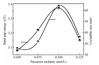
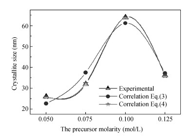
Table 1.
The experimental crystallite size

|
| [1] |
Benramache S, Rahal A, Benhaoua B. The effects of solvent nature on spray-deposited ZnO thin film prepared from Zn (CH3COO)2·2H2O. Optik, 2014, 125(2):663 doi: 10.1016/j.ijleo.2013.07.085
|
| [2] |
Benzarouk H, Drici A, Mekhnache M, et al. Effect of different dopant elements (Al, Mg and Ni) onmicrostructural, optical and electrochemical properties of ZnO thin films deposited by spray pyrolysis (SP). Superlattices and Microstructures, 2012, 52(3):594 doi: 10.1016/j.spmi.2012.06.007
|
| [3] |
Benramache S, Arif A, Belahssen O, et al. Study on the correlation between crystallite size and optical gap energy of doped ZnO thin film. Journal of Nanostructure in Chemistry, 2013, 3(80):1 doi: 10.1186/2193-8865-3-80?view=classic
|
| [4] |
Zhang Yong'ai, Wu Chaoxing, Zheng Yong, et al. Synthesis and efficient field emission characteristics of patterned ZnO nanowires. Journal of Semiconductors, 2012, 33(2):023001 doi: 10.1088/1674-4926/33/2/023001
|
| [5] |
Zhu Xiaming, Wu Huizhen, Wang Shuangjiang, et al. Optical and electrical properties of N-doped ZnO and fabrication of thin-film transistors. Journal of Semiconductors, 2009, 30(3):033001 doi: 10.1088/1674-4926/30/3/033001
|
| [6] |
Gahtar A, Benramache S, Benhaoua B, et al. Preparation of transparent conducting ZnO:Al films on glass substrates by ultrasonic spray technique. Journal of Semiconductors, 2013, 34(7):033001 http://www.jos.ac.cn/bdtxbcn/ch/reader/view_abstract.aspx?flag=1&file_no=12101001&journal_id=bdtxben
|
| [7] |
Ramana C V, Smith R J, Hussain O M. Grain size effects on the optical characteristics of pulsed-laser deposited vanadium oxide thin films. Phys Status Solidi A, 2003, 199(1):R4 doi: 10.1002/(ISSN)1521-396X
|
| [8] |
Bensouyad H, Adnane D, Dehdouh H, et al. Correlation between structural and optical properties of TiO2:ZnO thin films prepared by sol-gel method. Journal of Sol-Gel Sciences and Technology, 2011, 59(4):546 doi: 10.1007/s10971-011-2525-5
|
| [9] |
Ton-That C, Foley M, Phillips M R, et al. Correlation between the structural and optical properties of Mn-doped ZnO nanoparticles. Journal of Alloys and Compounds, 2012, 522(1):114 https://dro.deakin.edu.au/login.php?err=21&url=L2VzZXJ2L0RVOjMwMDQ5NjI3L3RzdXp1a2ktY29ycmVsYXRpb25iZXR3ZWVuLTIwMTIucGRm
|
| [10] |
Benramache S, Benhaoua B, Chabane F. Effect of substrate temperature on the stability of transparent conducting cobalt doped ZnO thin films. Journal of Semiconductors, 2012, 33(9):093001 doi: 10.1088/1674-4926/33/9/093001
|
| [11] |
Benramache S, Belahssen O, Guettaf A, et al. Correlation between electrical conductivity-optical band gap energy and precursor molarities ultrasonic spray deposition of ZnO thin films. Journal of Semiconductors, 2013, 34(11):113001 doi: 10.1088/1674-4926/34/11/113001
|
| [12] |
Wang S D, Miyadera T, Minari T, et al. Correlation between grain size and device parameters in pentacene thin film transistors. Appl Phys Lett, 2008, 93(4):043311 doi: 10.1063/1.2967193
|
| [13] |
Kappertz O, Drese R, Wuttig M. Correlation between structure, stress and deposition parameters in direct current sputtered zinc oxide films. J Vac Sci Technol A, 2002, 20(6):2084 doi: 10.1116/1.1517997
|
| [14] |
Wermelinger T, Mornaghini F C F, Hinderling C, et al. Correlation between the defect structure and the residual stress distribution in ZnO visualized by TEM and Raman microscopy. Mater Lett, 2010, 64(1):28 doi: 10.1016/j.matlet.2009.09.061
|
| [15] |
Zhu J J, Vines L, Aaltonen T, et al. Correlation between nitrogen and carbon incorporation into MOVPE ZnO at various oxidizing conditions. Microelectron J, 2009, 40(2):232 doi: 10.1016/j.mejo.2008.07.042
|
| [16] |
Tudose I V, Horvath P, Suchea M, et al. Correlation of ZnO thin film surface properties with conductivity. Appl Phys A, 2007, 89(1):57 doi: 10.1007/s00339-007-4036-3
|
| [17] |
Joshi B, Ghosh S, Srivastava P, et al. Correlation between electrical transport, microstructure and room temperature ferromagnetism in 200 keV Ni2+ ion implanted zinc oxide (ZnO) thin films. Appl Phys A, 2012, 107(2):393 doi: 10.1007/s00339-012-6785-x
|
| [18] |
Minami T, Nanto H, Takata S. Correlation between film quality and photoluminescence in sputtered ZnO thin films. J Mater Sci, 1982, 17(5):1364 doi: 10.1007/BF00752247
|
| [19] |
Nakanishi Y, Kato K, Omoto H, et al. Correlation between microstructure and salt-water durability of Ag thin films deposited by magnetron sputtering. Thin Solid Films, 2013, 532(1):141 http://www.sciencedirect.com/science/article/pii/S0040609013000199
|
| [20] |
Ajimsha R S, Das A K, Singh B N, et al. Correlation between electrical and optical properties of Cr:ZnO thin films grown by pulsed laser deposition. Physica B, 2011, 406(12):4578 http://adsabs.harvard.edu/abs/2011PhyB..406.4578A
|
| [21] |
Benramache S, Chabane F, Belahssen O, et al. Preparation and characterization of transparent conductive ZnO thin films by ultrasonic spray technique. J Sci Eng, 2013, 2(2):97 http://www.oricpub.com/SE-2-2-40.pdf
|
| [22] |
Vernardou D, Kenanakis G, Couris S, et al. The effect of growth time on the morphology of ZnO structures deposited on Si (100) by the aqueous chemical growth technique. J Crystal Growth, 2007, 308(2):105
|
| [23] |
Benramache S, Benhaoua B. Influence of substrate temperature and Cobalt concentration on structural and optical properties of ZnO thin films prepared by ultrasonic spray technique. Superlattices and Microstructures, 2012, 52(4):807 doi: 10.1016/j.spmi.2012.06.005
|
| [24] |
Benramache S, Chabane F, Benhaoua B, et al. Influence of growth time on crystalline structure, conductivity and optical properties of ZnO thin films. Journal of Semiconductors, 2013, 34(2):023001 doi: 10.1088/1674-4926/34/2/023001
|
| [25] |
Benramache S, Benhaoua B, Chabane F, et al. A comparative study on the nanocrystalline ZnO thin films prepared by ultrasonic spray and sol-gel method. Optik, 2013, 124(18):3221 doi: 10.1016/j.ijleo.2012.10.001
|
| [26] |
Benramache S, Benhaoua B. Influence of annealing temperature on structural and optical properties of ZnO:In thin films prepared by ultrasonic spray technique. Superlattices and Microstructures, 2012, 52(6):1062 doi: 10.1016/j.spmi.2012.08.006
|
| [27] |
Benramache S, Benhaoua B, Khechai N, et al. Elaboration and characterisation of ZnO thin films. Matériaux & Techniques, 2012, 100(6/7):573 http://www.mattech-journal.org/fr/articles/mattech/abs/2012/07/mt120017/mt120017.html
|
| [28] |
Zhang C. High-quality oriented ZnO films grown by sol-gel process assisted with ZnO. J Phys Chem Solids, 2010, 71(2):364
|
| [29] |
Subramanian M, Tanemura M, Hihara T, et al. Magnetic anisotropy in nanocrystalline Co-doped ZnO thin films. Chem Phys Lett, 2010, 487(1):97 http://cat.inist.fr/?aModele=afficheN&cpsidt=22448950
|
| [30] |
Li Y, Gong J, McCune M, et al. I-V characteristics of the p-n junction between vertically aligned ZnO nanorodsand polyaniline thin film. Synthetic Metals, 2010, 160(3):499
|
| [31] |
Jain A, Sagar P, Mehra R M. Band gap widening and narrowing in moderately and heavily doped n-ZnO films. Solid-State Electron, 2006, 50(2):1420 http://adsabs.harvard.edu/abs/2006SSEle..50.1420J
|


Article views: 4166 Times PDF downloads: 68 Times Cited by: 0 Times
Received: 14 October 2013 Revised: 24 November 2013 Online: Published: 01 April 2014
| Citation: |
S. Benramache, O. Belahssen, A. Guettaf, A. Arif. Correlation between crystallite size-optical gap energy and precursor molarities of ZnO thin films[J]. Journal of Semiconductors, 2014, 35(4): 042001. doi: 10.1088/1674-4926/35/4/042001
****
S. Benramache, O. Belahssen, A. Guettaf, A. Arif. Correlation between crystallite size-optical gap energy and precursor molarities of ZnO thin films[J]. J. Semicond., 2014, 35(4): 042001. doi: 10.1088/1674-4926/35/4/042001.

|
| [1] |
Benramache S, Rahal A, Benhaoua B. The effects of solvent nature on spray-deposited ZnO thin film prepared from Zn (CH3COO)2·2H2O. Optik, 2014, 125(2):663 doi: 10.1016/j.ijleo.2013.07.085
|
| [2] |
Benzarouk H, Drici A, Mekhnache M, et al. Effect of different dopant elements (Al, Mg and Ni) onmicrostructural, optical and electrochemical properties of ZnO thin films deposited by spray pyrolysis (SP). Superlattices and Microstructures, 2012, 52(3):594 doi: 10.1016/j.spmi.2012.06.007
|
| [3] |
Benramache S, Arif A, Belahssen O, et al. Study on the correlation between crystallite size and optical gap energy of doped ZnO thin film. Journal of Nanostructure in Chemistry, 2013, 3(80):1 doi: 10.1186/2193-8865-3-80?view=classic
|
| [4] |
Zhang Yong'ai, Wu Chaoxing, Zheng Yong, et al. Synthesis and efficient field emission characteristics of patterned ZnO nanowires. Journal of Semiconductors, 2012, 33(2):023001 doi: 10.1088/1674-4926/33/2/023001
|
| [5] |
Zhu Xiaming, Wu Huizhen, Wang Shuangjiang, et al. Optical and electrical properties of N-doped ZnO and fabrication of thin-film transistors. Journal of Semiconductors, 2009, 30(3):033001 doi: 10.1088/1674-4926/30/3/033001
|
| [6] |
Gahtar A, Benramache S, Benhaoua B, et al. Preparation of transparent conducting ZnO:Al films on glass substrates by ultrasonic spray technique. Journal of Semiconductors, 2013, 34(7):033001 http://www.jos.ac.cn/bdtxbcn/ch/reader/view_abstract.aspx?flag=1&file_no=12101001&journal_id=bdtxben
|
| [7] |
Ramana C V, Smith R J, Hussain O M. Grain size effects on the optical characteristics of pulsed-laser deposited vanadium oxide thin films. Phys Status Solidi A, 2003, 199(1):R4 doi: 10.1002/(ISSN)1521-396X
|
| [8] |
Bensouyad H, Adnane D, Dehdouh H, et al. Correlation between structural and optical properties of TiO2:ZnO thin films prepared by sol-gel method. Journal of Sol-Gel Sciences and Technology, 2011, 59(4):546 doi: 10.1007/s10971-011-2525-5
|
| [9] |
Ton-That C, Foley M, Phillips M R, et al. Correlation between the structural and optical properties of Mn-doped ZnO nanoparticles. Journal of Alloys and Compounds, 2012, 522(1):114 https://dro.deakin.edu.au/login.php?err=21&url=L2VzZXJ2L0RVOjMwMDQ5NjI3L3RzdXp1a2ktY29ycmVsYXRpb25iZXR3ZWVuLTIwMTIucGRm
|
| [10] |
Benramache S, Benhaoua B, Chabane F. Effect of substrate temperature on the stability of transparent conducting cobalt doped ZnO thin films. Journal of Semiconductors, 2012, 33(9):093001 doi: 10.1088/1674-4926/33/9/093001
|
| [11] |
Benramache S, Belahssen O, Guettaf A, et al. Correlation between electrical conductivity-optical band gap energy and precursor molarities ultrasonic spray deposition of ZnO thin films. Journal of Semiconductors, 2013, 34(11):113001 doi: 10.1088/1674-4926/34/11/113001
|
| [12] |
Wang S D, Miyadera T, Minari T, et al. Correlation between grain size and device parameters in pentacene thin film transistors. Appl Phys Lett, 2008, 93(4):043311 doi: 10.1063/1.2967193
|
| [13] |
Kappertz O, Drese R, Wuttig M. Correlation between structure, stress and deposition parameters in direct current sputtered zinc oxide films. J Vac Sci Technol A, 2002, 20(6):2084 doi: 10.1116/1.1517997
|
| [14] |
Wermelinger T, Mornaghini F C F, Hinderling C, et al. Correlation between the defect structure and the residual stress distribution in ZnO visualized by TEM and Raman microscopy. Mater Lett, 2010, 64(1):28 doi: 10.1016/j.matlet.2009.09.061
|
| [15] |
Zhu J J, Vines L, Aaltonen T, et al. Correlation between nitrogen and carbon incorporation into MOVPE ZnO at various oxidizing conditions. Microelectron J, 2009, 40(2):232 doi: 10.1016/j.mejo.2008.07.042
|
| [16] |
Tudose I V, Horvath P, Suchea M, et al. Correlation of ZnO thin film surface properties with conductivity. Appl Phys A, 2007, 89(1):57 doi: 10.1007/s00339-007-4036-3
|
| [17] |
Joshi B, Ghosh S, Srivastava P, et al. Correlation between electrical transport, microstructure and room temperature ferromagnetism in 200 keV Ni2+ ion implanted zinc oxide (ZnO) thin films. Appl Phys A, 2012, 107(2):393 doi: 10.1007/s00339-012-6785-x
|
| [18] |
Minami T, Nanto H, Takata S. Correlation between film quality and photoluminescence in sputtered ZnO thin films. J Mater Sci, 1982, 17(5):1364 doi: 10.1007/BF00752247
|
| [19] |
Nakanishi Y, Kato K, Omoto H, et al. Correlation between microstructure and salt-water durability of Ag thin films deposited by magnetron sputtering. Thin Solid Films, 2013, 532(1):141 http://www.sciencedirect.com/science/article/pii/S0040609013000199
|
| [20] |
Ajimsha R S, Das A K, Singh B N, et al. Correlation between electrical and optical properties of Cr:ZnO thin films grown by pulsed laser deposition. Physica B, 2011, 406(12):4578 http://adsabs.harvard.edu/abs/2011PhyB..406.4578A
|
| [21] |
Benramache S, Chabane F, Belahssen O, et al. Preparation and characterization of transparent conductive ZnO thin films by ultrasonic spray technique. J Sci Eng, 2013, 2(2):97 http://www.oricpub.com/SE-2-2-40.pdf
|
| [22] |
Vernardou D, Kenanakis G, Couris S, et al. The effect of growth time on the morphology of ZnO structures deposited on Si (100) by the aqueous chemical growth technique. J Crystal Growth, 2007, 308(2):105
|
| [23] |
Benramache S, Benhaoua B. Influence of substrate temperature and Cobalt concentration on structural and optical properties of ZnO thin films prepared by ultrasonic spray technique. Superlattices and Microstructures, 2012, 52(4):807 doi: 10.1016/j.spmi.2012.06.005
|
| [24] |
Benramache S, Chabane F, Benhaoua B, et al. Influence of growth time on crystalline structure, conductivity and optical properties of ZnO thin films. Journal of Semiconductors, 2013, 34(2):023001 doi: 10.1088/1674-4926/34/2/023001
|
| [25] |
Benramache S, Benhaoua B, Chabane F, et al. A comparative study on the nanocrystalline ZnO thin films prepared by ultrasonic spray and sol-gel method. Optik, 2013, 124(18):3221 doi: 10.1016/j.ijleo.2012.10.001
|
| [26] |
Benramache S, Benhaoua B. Influence of annealing temperature on structural and optical properties of ZnO:In thin films prepared by ultrasonic spray technique. Superlattices and Microstructures, 2012, 52(6):1062 doi: 10.1016/j.spmi.2012.08.006
|
| [27] |
Benramache S, Benhaoua B, Khechai N, et al. Elaboration and characterisation of ZnO thin films. Matériaux & Techniques, 2012, 100(6/7):573 http://www.mattech-journal.org/fr/articles/mattech/abs/2012/07/mt120017/mt120017.html
|
| [28] |
Zhang C. High-quality oriented ZnO films grown by sol-gel process assisted with ZnO. J Phys Chem Solids, 2010, 71(2):364
|
| [29] |
Subramanian M, Tanemura M, Hihara T, et al. Magnetic anisotropy in nanocrystalline Co-doped ZnO thin films. Chem Phys Lett, 2010, 487(1):97 http://cat.inist.fr/?aModele=afficheN&cpsidt=22448950
|
| [30] |
Li Y, Gong J, McCune M, et al. I-V characteristics of the p-n junction between vertically aligned ZnO nanorodsand polyaniline thin film. Synthetic Metals, 2010, 160(3):499
|
| [31] |
Jain A, Sagar P, Mehra R M. Band gap widening and narrowing in moderately and heavily doped n-ZnO films. Solid-State Electron, 2006, 50(2):1420 http://adsabs.harvard.edu/abs/2006SSEle..50.1420J
|

 WeChat ID
Journal of Semiconductors © 2017 All Rights Reserved 京ICP备05085259号-2

 DownLoad: