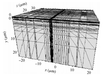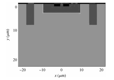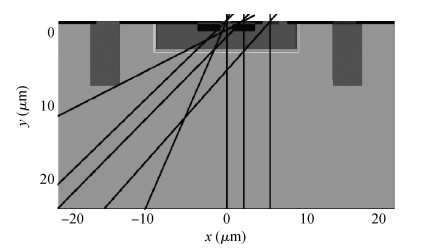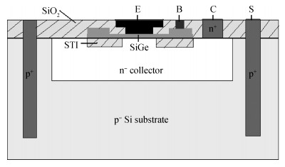
Fig. 1.
Schematic device cross section of SiGe HBT.
SEMICONDUCTOR DEVICES
Jinxin Zhang1, 3, Hongxia Guo1, 2, , Lin Wen1, 3, Qi Guo1, Jiangwei Cui1, Xin Wang1, 3, Wei Deng1, 3, Qiwen Zhen1, 3, Xue Fan4 and Yao Xiao2
Corresponding author: Guo Hongxia, Email: guohxnint@yahoo.cn
Abstract: This paper presents 3-D simulation of angled strike heavy-ion induced charge collection in domestic silicon-germanium heterojunction bipolar transistors (SiGe HBTs). 3D damaged model of SiGe HBTs single-event effects (SEE) is built by TCAD simulation tools to research ions angled strike dependence. We select several different strike angles at variously typical ions strike positions. The charge collection mechanism for each terminal is identified based on analysis of the device structure and simulation results. Charge collection induced by angled strike ions presents a complex situation. Whether the location of device ions enters, as long as ions track through the sensitive volume, it will cause vast charge collection. The amount of charge collection of SiGe HBT is not only related to length of ions track in sensitive volume, but also influenced by STI and distance between ions track and electrodes. The simulation model is useful to research the practical applications of SiGe HBTs in space, and provides a theoretical basis for the further radiation hardening.
Keywords: SiGe heterojunction bipolar transistors, single-event effects, angled strike, three-dimensional numerical simulation
| [1] |
Cressler J D. SiGe HBT technology:a new contender for Si-based RF and microwave circuit applications. IEEE Trans Microwave Theory Tech, 1998, 46(5):572 doi: 10.1109/22.668665
|
| [2] |
Cressler J D. On the potential of SiGe HBTs for extreme environment electronics. Proc IEEE, 2005, 93(9):1559 doi: 10.1109/JPROC.2005.852225
|
| [3] |
Cressler J D. Radiation effects in SiGe HBT BiCMOS technology. IEEE Nuclear and Space Radiation Effects Conference Short Course Note Book, 2003, Section Ⅴ http://ieeexplore.ieee.org/xpl/abstractKeywords.jsp?reload=true&arnumber=6484205&filter%3DAND%28p_IS_Number%3A6530644%29
|
| [4] |
Diestelhorst R M. Silicon-germanium BiCMOS device and circuit design for extreme environment applications. Master Dissertation, Georgia Institute of Technology, Georgia, USA, 2009 https://smartech.gatech.edu/handle/1853/28180?show=full
|
| [5] |
Appaswamy A. Operation of inverse mode SiGe HBTs and ultra-scaled CMOS devices in extreme environments. PhD Dissertation, Georgia Institute of Technology, Georgia, USA, 2010 http://gradworks.umi.com/34/14/3414435.html
|
| [6] |
Wen J C, Shi R Y, Gong M, et al. Gamma irradiation effects on collector current and Early voltage of SiGe heterjunction bipolar transistor. High Power Laser and Particle Beams, 2011, 23(2):545 doi: 10.3788/HPLPB
|
| [7] |
Chen T B, Sutton A K, Bellini M, et al. Proton radiation effects in vertical SiGe HBTs fabricated on CMOS-compatible SOI. IEEE Trans Nucl Sci, 2005, 52(6):2353 doi: 10.1109/TNS.2005.860726
|
| [8] |
Niu Z H, Guo Q, Ren D Y, et al. Total dose Gamma irradiation effect an annealing characteristic of SiGe HBT. Chinese Journal of Semiconductors, 2006, 27(9):1608 http://www.oalib.com/paper/1523059#.WcR6f1Mdj3Q
|
| [9] |
Yang H. 3D device simulation of SEU-induced charge collection in 200 GHz SiGe HBTs. Master Dissertation, Auburn University, Alabama, USA, 2005 https://etd.auburn.edu/handle/10415/402
|
| [10] |
Varadharajaperumal M. 3D simulation of SEU in SiGe HBTS and radiation hardening by design. PhD Dissertation, Auburn University, Alabama, USA, 2010 https://etd.auburn.edu/handle/10415/2247?show=full
|
| [11] |
Niu G, Yang H, Varadharajaperumal M, et al. Simulation of a new back junction approach for reducing charge collection in 200 GHz SiGe HBTs. IEEE Trans Nucl Sci, 2005, 52(6):2153 doi: 10.1109/TNS.2005.860744
|
| [12] |
Pellish J A. Bulk silicon-germanium heterojunction bipolar transistor process feature implications for single-event effects analysis and charge collection mechanisms. PhD Dissertation, Vanderbilt University, Tennessee, USA, 2008 http://gradworks.umi.com/34/42/3442404.html
|
| [13] |
Duerr W, Menzel W, Schumacher H, et al. A low-noise active receiving antenna using a SiGe HBT. IEEE Microw Guided Wave Lett, 1997, 7(3):63 doi: 10.1109/75.556033
|
| [14] |
Varadharajaperumal M, Niu G, Wei X, et al. 3-D simulation of SEU hardening of SiGe HBTs using shared dummy collector. IEEE Trans Nucl Sci, 2007, 54(6):2330 doi: 10.1109/TNS.2007.910290
|
| [15] |
Zhang T. Impact of charge collection mechanisms on single event effects in SiGe HBT circuits and hardening implications. Master Dissertation, Auburn University, Alabama, USA, 2009
|
| [16] |
Shi Y. Design and optimization of nano-scaled silicon-germanium heterojunction bipolar transistors. PhD Dissertation, Auburn University, Alabama, USA, 2005 https://etd.auburn.edu/handle/10415/760
|
| [17] |
Pratapgarhwala M M. Characterization of transistor matching in silicon-germanium heterojunction bipolar transistors. Master Dissertation, Georgia Institute of Technology, Georgia, USA, 2005 https://smartech.gatech.edu/bitstream/handle/1853/7536/Pratapgarhwala_Mustansir_M_200512_MS.pdf?sequence=1
|
| [18] |
Shi Y. Design and optimization of nano-scaled silicon-germanium heterojunction bipolar transistors. PhD Dissertation, Auburn University, Alabama, USA, 2005 https://etd.auburn.edu/handle/10415/760
|
| [19] |
Cressler J D. Using SiGe technology in extreme environments. NASA NEPP Electronics Technology Workshop, 2010 http://yadda.icm.edu.pl/yadda/element/bwmeta1.element.ieee-000004422235
|
| [20] |
Kuo W M L, Krithivasan R, Li X, et al. A low power, X-band SiGe HBT low noise amplifier for near-space radar applications. IEEE Microw Wireless Computer Lett, 2006, 16(9):520 doi: 10.1109/LMWC.2006.880696
|
Table 1. The simulated charge collection of angled strike.

|
| [1] |
Cressler J D. SiGe HBT technology:a new contender for Si-based RF and microwave circuit applications. IEEE Trans Microwave Theory Tech, 1998, 46(5):572 doi: 10.1109/22.668665
|
| [2] |
Cressler J D. On the potential of SiGe HBTs for extreme environment electronics. Proc IEEE, 2005, 93(9):1559 doi: 10.1109/JPROC.2005.852225
|
| [3] |
Cressler J D. Radiation effects in SiGe HBT BiCMOS technology. IEEE Nuclear and Space Radiation Effects Conference Short Course Note Book, 2003, Section Ⅴ http://ieeexplore.ieee.org/xpl/abstractKeywords.jsp?reload=true&arnumber=6484205&filter%3DAND%28p_IS_Number%3A6530644%29
|
| [4] |
Diestelhorst R M. Silicon-germanium BiCMOS device and circuit design for extreme environment applications. Master Dissertation, Georgia Institute of Technology, Georgia, USA, 2009 https://smartech.gatech.edu/handle/1853/28180?show=full
|
| [5] |
Appaswamy A. Operation of inverse mode SiGe HBTs and ultra-scaled CMOS devices in extreme environments. PhD Dissertation, Georgia Institute of Technology, Georgia, USA, 2010 http://gradworks.umi.com/34/14/3414435.html
|
| [6] |
Wen J C, Shi R Y, Gong M, et al. Gamma irradiation effects on collector current and Early voltage of SiGe heterjunction bipolar transistor. High Power Laser and Particle Beams, 2011, 23(2):545 doi: 10.3788/HPLPB
|
| [7] |
Chen T B, Sutton A K, Bellini M, et al. Proton radiation effects in vertical SiGe HBTs fabricated on CMOS-compatible SOI. IEEE Trans Nucl Sci, 2005, 52(6):2353 doi: 10.1109/TNS.2005.860726
|
| [8] |
Niu Z H, Guo Q, Ren D Y, et al. Total dose Gamma irradiation effect an annealing characteristic of SiGe HBT. Chinese Journal of Semiconductors, 2006, 27(9):1608 http://www.oalib.com/paper/1523059#.WcR6f1Mdj3Q
|
| [9] |
Yang H. 3D device simulation of SEU-induced charge collection in 200 GHz SiGe HBTs. Master Dissertation, Auburn University, Alabama, USA, 2005 https://etd.auburn.edu/handle/10415/402
|
| [10] |
Varadharajaperumal M. 3D simulation of SEU in SiGe HBTS and radiation hardening by design. PhD Dissertation, Auburn University, Alabama, USA, 2010 https://etd.auburn.edu/handle/10415/2247?show=full
|
| [11] |
Niu G, Yang H, Varadharajaperumal M, et al. Simulation of a new back junction approach for reducing charge collection in 200 GHz SiGe HBTs. IEEE Trans Nucl Sci, 2005, 52(6):2153 doi: 10.1109/TNS.2005.860744
|
| [12] |
Pellish J A. Bulk silicon-germanium heterojunction bipolar transistor process feature implications for single-event effects analysis and charge collection mechanisms. PhD Dissertation, Vanderbilt University, Tennessee, USA, 2008 http://gradworks.umi.com/34/42/3442404.html
|
| [13] |
Duerr W, Menzel W, Schumacher H, et al. A low-noise active receiving antenna using a SiGe HBT. IEEE Microw Guided Wave Lett, 1997, 7(3):63 doi: 10.1109/75.556033
|
| [14] |
Varadharajaperumal M, Niu G, Wei X, et al. 3-D simulation of SEU hardening of SiGe HBTs using shared dummy collector. IEEE Trans Nucl Sci, 2007, 54(6):2330 doi: 10.1109/TNS.2007.910290
|
| [15] |
Zhang T. Impact of charge collection mechanisms on single event effects in SiGe HBT circuits and hardening implications. Master Dissertation, Auburn University, Alabama, USA, 2009
|
| [16] |
Shi Y. Design and optimization of nano-scaled silicon-germanium heterojunction bipolar transistors. PhD Dissertation, Auburn University, Alabama, USA, 2005 https://etd.auburn.edu/handle/10415/760
|
| [17] |
Pratapgarhwala M M. Characterization of transistor matching in silicon-germanium heterojunction bipolar transistors. Master Dissertation, Georgia Institute of Technology, Georgia, USA, 2005 https://smartech.gatech.edu/bitstream/handle/1853/7536/Pratapgarhwala_Mustansir_M_200512_MS.pdf?sequence=1
|
| [18] |
Shi Y. Design and optimization of nano-scaled silicon-germanium heterojunction bipolar transistors. PhD Dissertation, Auburn University, Alabama, USA, 2005 https://etd.auburn.edu/handle/10415/760
|
| [19] |
Cressler J D. Using SiGe technology in extreme environments. NASA NEPP Electronics Technology Workshop, 2010 http://yadda.icm.edu.pl/yadda/element/bwmeta1.element.ieee-000004422235
|
| [20] |
Kuo W M L, Krithivasan R, Li X, et al. A low power, X-band SiGe HBT low noise amplifier for near-space radar applications. IEEE Microw Wireless Computer Lett, 2006, 16(9):520 doi: 10.1109/LMWC.2006.880696
|


Article views: 3118 Times PDF downloads: 23 Times Cited by: 0 Times
Received: 08 September 2013 Revised: 21 November 2013 Online: Published: 01 April 2014
| Citation: |
Jinxin Zhang, Hongxia Guo, Lin Wen, Qi Guo, Jiangwei Cui, Xin Wang, Wei Deng, Qiwen Zhen, Xue Fan, Yao Xiao. 3-D simulation of angled strike heavy-ion induced charge collection in silicon-germanium heterojunction bipolar transistors[J]. Journal of Semiconductors, 2014, 35(4): 044003. doi: 10.1088/1674-4926/35/4/044003
****
J X Zhang, H X Guo, L Wen, Q Guo, J W Cui, X Wang, W Deng, Q W Zhen, X Fan, Y Xiao. 3-D simulation of angled strike heavy-ion induced charge collection in silicon-germanium heterojunction bipolar transistors[J]. J. Semicond., 2014, 35(4): 044003. doi: 10.1088/1674-4926/35/4/044003.

|
| [1] |
Cressler J D. SiGe HBT technology:a new contender for Si-based RF and microwave circuit applications. IEEE Trans Microwave Theory Tech, 1998, 46(5):572 doi: 10.1109/22.668665
|
| [2] |
Cressler J D. On the potential of SiGe HBTs for extreme environment electronics. Proc IEEE, 2005, 93(9):1559 doi: 10.1109/JPROC.2005.852225
|
| [3] |
Cressler J D. Radiation effects in SiGe HBT BiCMOS technology. IEEE Nuclear and Space Radiation Effects Conference Short Course Note Book, 2003, Section Ⅴ http://ieeexplore.ieee.org/xpl/abstractKeywords.jsp?reload=true&arnumber=6484205&filter%3DAND%28p_IS_Number%3A6530644%29
|
| [4] |
Diestelhorst R M. Silicon-germanium BiCMOS device and circuit design for extreme environment applications. Master Dissertation, Georgia Institute of Technology, Georgia, USA, 2009 https://smartech.gatech.edu/handle/1853/28180?show=full
|
| [5] |
Appaswamy A. Operation of inverse mode SiGe HBTs and ultra-scaled CMOS devices in extreme environments. PhD Dissertation, Georgia Institute of Technology, Georgia, USA, 2010 http://gradworks.umi.com/34/14/3414435.html
|
| [6] |
Wen J C, Shi R Y, Gong M, et al. Gamma irradiation effects on collector current and Early voltage of SiGe heterjunction bipolar transistor. High Power Laser and Particle Beams, 2011, 23(2):545 doi: 10.3788/HPLPB
|
| [7] |
Chen T B, Sutton A K, Bellini M, et al. Proton radiation effects in vertical SiGe HBTs fabricated on CMOS-compatible SOI. IEEE Trans Nucl Sci, 2005, 52(6):2353 doi: 10.1109/TNS.2005.860726
|
| [8] |
Niu Z H, Guo Q, Ren D Y, et al. Total dose Gamma irradiation effect an annealing characteristic of SiGe HBT. Chinese Journal of Semiconductors, 2006, 27(9):1608 http://www.oalib.com/paper/1523059#.WcR6f1Mdj3Q
|
| [9] |
Yang H. 3D device simulation of SEU-induced charge collection in 200 GHz SiGe HBTs. Master Dissertation, Auburn University, Alabama, USA, 2005 https://etd.auburn.edu/handle/10415/402
|
| [10] |
Varadharajaperumal M. 3D simulation of SEU in SiGe HBTS and radiation hardening by design. PhD Dissertation, Auburn University, Alabama, USA, 2010 https://etd.auburn.edu/handle/10415/2247?show=full
|
| [11] |
Niu G, Yang H, Varadharajaperumal M, et al. Simulation of a new back junction approach for reducing charge collection in 200 GHz SiGe HBTs. IEEE Trans Nucl Sci, 2005, 52(6):2153 doi: 10.1109/TNS.2005.860744
|
| [12] |
Pellish J A. Bulk silicon-germanium heterojunction bipolar transistor process feature implications for single-event effects analysis and charge collection mechanisms. PhD Dissertation, Vanderbilt University, Tennessee, USA, 2008 http://gradworks.umi.com/34/42/3442404.html
|
| [13] |
Duerr W, Menzel W, Schumacher H, et al. A low-noise active receiving antenna using a SiGe HBT. IEEE Microw Guided Wave Lett, 1997, 7(3):63 doi: 10.1109/75.556033
|
| [14] |
Varadharajaperumal M, Niu G, Wei X, et al. 3-D simulation of SEU hardening of SiGe HBTs using shared dummy collector. IEEE Trans Nucl Sci, 2007, 54(6):2330 doi: 10.1109/TNS.2007.910290
|
| [15] |
Zhang T. Impact of charge collection mechanisms on single event effects in SiGe HBT circuits and hardening implications. Master Dissertation, Auburn University, Alabama, USA, 2009
|
| [16] |
Shi Y. Design and optimization of nano-scaled silicon-germanium heterojunction bipolar transistors. PhD Dissertation, Auburn University, Alabama, USA, 2005 https://etd.auburn.edu/handle/10415/760
|
| [17] |
Pratapgarhwala M M. Characterization of transistor matching in silicon-germanium heterojunction bipolar transistors. Master Dissertation, Georgia Institute of Technology, Georgia, USA, 2005 https://smartech.gatech.edu/bitstream/handle/1853/7536/Pratapgarhwala_Mustansir_M_200512_MS.pdf?sequence=1
|
| [18] |
Shi Y. Design and optimization of nano-scaled silicon-germanium heterojunction bipolar transistors. PhD Dissertation, Auburn University, Alabama, USA, 2005 https://etd.auburn.edu/handle/10415/760
|
| [19] |
Cressler J D. Using SiGe technology in extreme environments. NASA NEPP Electronics Technology Workshop, 2010 http://yadda.icm.edu.pl/yadda/element/bwmeta1.element.ieee-000004422235
|
| [20] |
Kuo W M L, Krithivasan R, Li X, et al. A low power, X-band SiGe HBT low noise amplifier for near-space radar applications. IEEE Microw Wireless Computer Lett, 2006, 16(9):520 doi: 10.1109/LMWC.2006.880696
|

 WeChat ID
Journal of Semiconductors © 2017 All Rights Reserved 京ICP备05085259号-2

 DownLoad: