


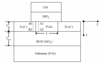
Fig. 1.
The schematic structure of a GeOI MOSFET.
SEMICONDUCTOR DEVICES
Minmin Fan, Jingping Xu, Lu Liu and Yurong Bai
Corresponding author: Xu Jingping, Email: jpxu@mail.hust.edu.cn
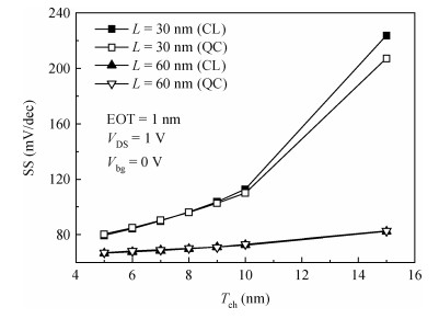
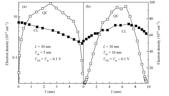
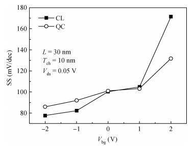
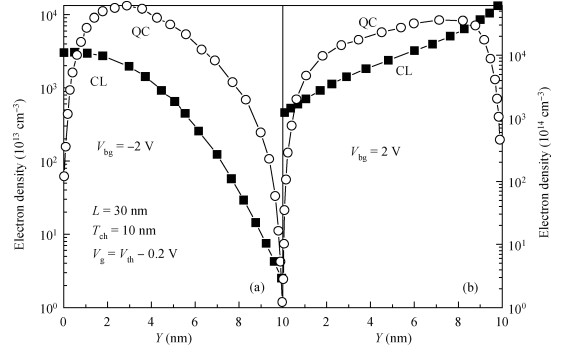
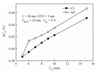
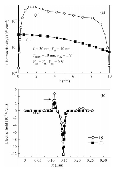
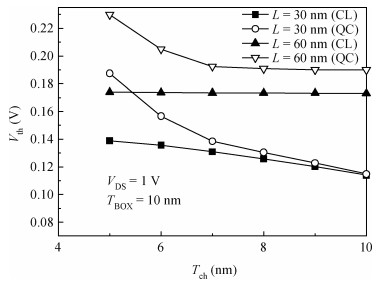
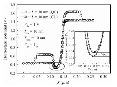
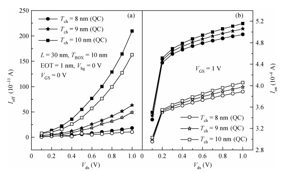
Abstract: The impact of quantum confinement on the electrical characteristics of ultrathin-channel GeOI n-MOSFETs is investigated on the basis of the density-gradient model in TCAD software. The effects of the channel thickness (Tch) and back-gate bias (Vbg) on the electrical characteristics of GeOI MOSFETs are examined, and the simulated results are compared with those using the conventional semi-classical model. It is shown that when Tch > 8 nm, the electron conduction path of the GeOI MOSFET is closer to the front-gate interface under the QC model than under the CL model, and vice versa when Tch < 8 nm. Thus the electrically controlled ability of the front gate of the devices is influenced by the quantum effect. In addition, the quantum-mechanical mechanism will enhance the drain-induced barrier lowering effect, increase the threshold voltage and decrease the on-state current; for a short channel length (≤ 30 nm), when Tch > 8 nm(or < 8 nm), the quantum-mechanical mechanism mainly impacts the subthreshold slope (or the threshold voltage). Due to the quantum-size effect, the off-state current can be suppressed as the channel thickness decreases.
Keywords: GeOI MOSFET, quantum confinement, subthreshold slope, threshold voltage
| [1] |
Frank D J, Dennard R H, Nowak E, et al. Device scaling limits of Si MOSFETs and their application dependencies. Proc IEEE, 2001, 89(3):259 doi: 10.1109/5.915374
|
| [2] |
Sharma R, Pandey S, Jain S B. Analytical modeling of drain current and RF performance for double gate fully depleted nano-scale SOI MOSFETS. Journal of Semiconductors, 2012, 33(2):024001 doi: 10.1088/1674-4926/33/2/024001
|
| [3] |
Choi Y K, Asano K, Lindert N, et al. Ultrathin-body SOI MOSFET for deep-sub-tenth micro era. IEEE Electron Device Lett, 2000, 21(5):254 doi: 10.1109/55.841313
|
| [4] |
Hu Aibin, Xu Qiuxia. Effects of silicon nitride diffusion barrier on germanium MOS capacitors with HfON gate dielectrics. Journal of Semiconductors, 2009, 30(10):104002 doi: 10.1088/1674-4926/30/10/104002
|
| [5] |
Le Royer C, Clavelier L, Tabone C, et al. 105 nm gate length pMOSFETs with high-k and metal gate fabricated in a Si process line on 200 mm GeOI wafers. Solid-State Electron, 2008, 52(9):1285 doi: 10.1016/j.sse.2008.04.019
|
| [6] |
De Jaeger B, Kaczer B, Zimmerman P, et al. Ge deep sub-micron HiK/MG pFETs with superior drive compared to Si HiK/MG state-of-the-art reference. Semicond Sci Technol, 2007, 22(1):S221 doi: 10.1088/0268-1242/22/1/S52
|
| [7] |
Pop E, Chui C O, Dutton R, et al. Electro-thermal comparison and performance optimization of thin-body SOI and GOI MOSFETs. IEEE International Electron Devices Meeting, IEDM Technical Digest, 2004:411 http://ieeexplore.ieee.org/iel5/9719/30682/01419172.pdf
|
| [8] |
Bedell S W, Majumdar A, Ott J A, et al. Mobility scaling in short-channel length strained Ge-on-insulator P-MOSFETs. IEEE Electron Device Lett, 2008, 29(7):811 doi: 10.1109/LED.2008.2000713
|
| [9] |
Pala M, Le Royer C, Le Carval G, et al. Modeling of non-equilibrium transport effects in Fully-Depleted GeOI-MOSFETs. Journal of Computational Electronics, 2006, 5(2/3):241 doi: 10.1007/s10825-006-8851-0
|
| [10] |
Grandchamp B, Jaud M A, Scheiblin P, et al. In-depth physical investigation of GeOI pMOSFET by TCAD calibrated simulation. Solid-State Electron, 2011, 57(1):67 doi: 10.1016/j.sse.2010.11.011
|
| [11] |
Yu C H, Wu Y S, Hu V P H, et al. Impact of quantum confinement on backgate-bias modulated threshold-voltage and subthreshold characteristics for ultra-thin-body GeOI MOSFETs. IEEE Trans Electron Devices, 2012, 59(7):1851 doi: 10.1109/TED.2012.2194499
|
| [12] |
Yu C H, Wu Y S, Hu V P H, et al. Impact of quantum confinement on subthreshold swing and electrostatic integrity of ultra-thin-body GeOI and InGaAs-OI n-MOSFETs. IEEE Trans Nanotechnology, 2012, 11(2):287 doi: 10.1109/TNANO.2011.2169084
|
| [13] |
Wu Y S, Hsieh H Y, Hu V P H, et al. Impact of quantum confinement on short-channel effects for ultrathin-body germanium-on-insulator MOSFETs. IEEE Electron Device Lett, 2011, 32(1):18 doi: 10.1109/LED.2010.2089425
|
| [14] |
Omura Y, Konishi H, Sato S. Quantum-mechanical suppression and enhancement of SCEs in ultrathin SOI MOSFETs. IEEE Trans Electron Devices, 2006, 53(4):677 doi: 10.1109/TED.2006.870274
|
| [15] |
Ancona M G, Tiersten H F. Macroscopic physics of the silicon inversion layer. Phys Rev B, Condens Matter, 1987, 35(15):7959 doi: 10.1103/PhysRevB.35.7959
|
| [16] |
Ancona M G, Iafrate G J. Quantum correction to the equation of state of an electron gas in a semiconductor. Phys Rev B, Condens Matter, 1989, 39(13):9536 doi: 10.1103/PhysRevB.39.9536
|
| [17] |
Wettstein A, Schenk A, Fichtner W. Quantum device-simulation with the density-gradient model on unstructured grids. IEEE Trans Electron Devices, 2001, 48(2):279 doi: 10.1109/16.902727
|
| [18] |
Lombardi C, Manzini S, Saporito A, et al. A physically based mobility model for numerical simulation of nonplanar devices. IEEE Trans Computer-Aided Design of Integrated Circuits and Systems, 1988, 7(11):1164 doi: 10.1109/43.9186
|
| [19] |
Shapiro S D. Carrier mobilities m silicon empirically related to doping and field. Proc IEEE, 1967 http://ieeexplore.ieee.org/xpl/abstractKeywords.jsp?arnumber=1448053
|
| [20] |
Van Den Daele W, Augendre E, Le Royer C, et al. Low-temperature characterization and modeling of advanced GeOI pMOSFETs:mobility mechanisms and origin of the parasitic conduction. Solid-State Electron, 2010, 54(2):205 doi: 10.1016/j.sse.2009.12.020
|
| [21] |
Omura Y, Ishiyama T, Shoji M, et al. Quantum mechanical transport characteristics in ultimately miniaturized MOSFETs/SIMOX. Proceedings of the 10th International Symposium on SOI Technology and Development, 1996:199
|
| [22] |
Hu V P H, Fan M L, Su P, et al. Band-to-band-tunneling leakage suppression for ultra-thin-body GeOI MOSFETs using transistor stacking. IEEE Electron Device Lett, 2012, 33(2):197 doi: 10.1109/LED.2011.2177955
|
| [23] |
Hu V P H, Fan M L, Su P, et al. Leakage-delay analysis of ultra-thin-body GeOI devices and logic circuits. IEEE International Symposium on VLSI Technology, Systems and Applications (VLSI-TSA), 2011:1 http://ieeexplore.ieee.org/xpl/articleDetails.jsp?tp=&arnumber=5872220&contentType=Conference+Publications&sortType%3Dasc_p_Sequence%26filter%3DAND%28p_IS_Number%3A5872202%29
|


Article views: 2998 Times PDF downloads: 36 Times Cited by: 0 Times
Received: 16 September 2013 Revised: 08 November 2013 Online: Published: 01 April 2014
| Citation: |
Minmin Fan, Jingping Xu, Lu Liu, Yurong Bai. The impact of quantum confinement on the electrical characteristics of ultrathin-channel GeOI MOSFETs[J]. Journal of Semiconductors, 2014, 35(4): 044004. doi: 10.1088/1674-4926/35/4/044004
****
M M Fan, J P Xu, L Liu, Y R Bai. The impact of quantum confinement on the electrical characteristics of ultrathin-channel GeOI MOSFETs[J]. J. Semicond., 2014, 35(4): 044004. doi: 10.1088/1674-4926/35/4/044004.

|
| [1] |
Frank D J, Dennard R H, Nowak E, et al. Device scaling limits of Si MOSFETs and their application dependencies. Proc IEEE, 2001, 89(3):259 doi: 10.1109/5.915374
|
| [2] |
Sharma R, Pandey S, Jain S B. Analytical modeling of drain current and RF performance for double gate fully depleted nano-scale SOI MOSFETS. Journal of Semiconductors, 2012, 33(2):024001 doi: 10.1088/1674-4926/33/2/024001
|
| [3] |
Choi Y K, Asano K, Lindert N, et al. Ultrathin-body SOI MOSFET for deep-sub-tenth micro era. IEEE Electron Device Lett, 2000, 21(5):254 doi: 10.1109/55.841313
|
| [4] |
Hu Aibin, Xu Qiuxia. Effects of silicon nitride diffusion barrier on germanium MOS capacitors with HfON gate dielectrics. Journal of Semiconductors, 2009, 30(10):104002 doi: 10.1088/1674-4926/30/10/104002
|
| [5] |
Le Royer C, Clavelier L, Tabone C, et al. 105 nm gate length pMOSFETs with high-k and metal gate fabricated in a Si process line on 200 mm GeOI wafers. Solid-State Electron, 2008, 52(9):1285 doi: 10.1016/j.sse.2008.04.019
|
| [6] |
De Jaeger B, Kaczer B, Zimmerman P, et al. Ge deep sub-micron HiK/MG pFETs with superior drive compared to Si HiK/MG state-of-the-art reference. Semicond Sci Technol, 2007, 22(1):S221 doi: 10.1088/0268-1242/22/1/S52
|
| [7] |
Pop E, Chui C O, Dutton R, et al. Electro-thermal comparison and performance optimization of thin-body SOI and GOI MOSFETs. IEEE International Electron Devices Meeting, IEDM Technical Digest, 2004:411 http://ieeexplore.ieee.org/iel5/9719/30682/01419172.pdf
|
| [8] |
Bedell S W, Majumdar A, Ott J A, et al. Mobility scaling in short-channel length strained Ge-on-insulator P-MOSFETs. IEEE Electron Device Lett, 2008, 29(7):811 doi: 10.1109/LED.2008.2000713
|
| [9] |
Pala M, Le Royer C, Le Carval G, et al. Modeling of non-equilibrium transport effects in Fully-Depleted GeOI-MOSFETs. Journal of Computational Electronics, 2006, 5(2/3):241 doi: 10.1007/s10825-006-8851-0
|
| [10] |
Grandchamp B, Jaud M A, Scheiblin P, et al. In-depth physical investigation of GeOI pMOSFET by TCAD calibrated simulation. Solid-State Electron, 2011, 57(1):67 doi: 10.1016/j.sse.2010.11.011
|
| [11] |
Yu C H, Wu Y S, Hu V P H, et al. Impact of quantum confinement on backgate-bias modulated threshold-voltage and subthreshold characteristics for ultra-thin-body GeOI MOSFETs. IEEE Trans Electron Devices, 2012, 59(7):1851 doi: 10.1109/TED.2012.2194499
|
| [12] |
Yu C H, Wu Y S, Hu V P H, et al. Impact of quantum confinement on subthreshold swing and electrostatic integrity of ultra-thin-body GeOI and InGaAs-OI n-MOSFETs. IEEE Trans Nanotechnology, 2012, 11(2):287 doi: 10.1109/TNANO.2011.2169084
|
| [13] |
Wu Y S, Hsieh H Y, Hu V P H, et al. Impact of quantum confinement on short-channel effects for ultrathin-body germanium-on-insulator MOSFETs. IEEE Electron Device Lett, 2011, 32(1):18 doi: 10.1109/LED.2010.2089425
|
| [14] |
Omura Y, Konishi H, Sato S. Quantum-mechanical suppression and enhancement of SCEs in ultrathin SOI MOSFETs. IEEE Trans Electron Devices, 2006, 53(4):677 doi: 10.1109/TED.2006.870274
|
| [15] |
Ancona M G, Tiersten H F. Macroscopic physics of the silicon inversion layer. Phys Rev B, Condens Matter, 1987, 35(15):7959 doi: 10.1103/PhysRevB.35.7959
|
| [16] |
Ancona M G, Iafrate G J. Quantum correction to the equation of state of an electron gas in a semiconductor. Phys Rev B, Condens Matter, 1989, 39(13):9536 doi: 10.1103/PhysRevB.39.9536
|
| [17] |
Wettstein A, Schenk A, Fichtner W. Quantum device-simulation with the density-gradient model on unstructured grids. IEEE Trans Electron Devices, 2001, 48(2):279 doi: 10.1109/16.902727
|
| [18] |
Lombardi C, Manzini S, Saporito A, et al. A physically based mobility model for numerical simulation of nonplanar devices. IEEE Trans Computer-Aided Design of Integrated Circuits and Systems, 1988, 7(11):1164 doi: 10.1109/43.9186
|
| [19] |
Shapiro S D. Carrier mobilities m silicon empirically related to doping and field. Proc IEEE, 1967 http://ieeexplore.ieee.org/xpl/abstractKeywords.jsp?arnumber=1448053
|
| [20] |
Van Den Daele W, Augendre E, Le Royer C, et al. Low-temperature characterization and modeling of advanced GeOI pMOSFETs:mobility mechanisms and origin of the parasitic conduction. Solid-State Electron, 2010, 54(2):205 doi: 10.1016/j.sse.2009.12.020
|
| [21] |
Omura Y, Ishiyama T, Shoji M, et al. Quantum mechanical transport characteristics in ultimately miniaturized MOSFETs/SIMOX. Proceedings of the 10th International Symposium on SOI Technology and Development, 1996:199
|
| [22] |
Hu V P H, Fan M L, Su P, et al. Band-to-band-tunneling leakage suppression for ultra-thin-body GeOI MOSFETs using transistor stacking. IEEE Electron Device Lett, 2012, 33(2):197 doi: 10.1109/LED.2011.2177955
|
| [23] |
Hu V P H, Fan M L, Su P, et al. Leakage-delay analysis of ultra-thin-body GeOI devices and logic circuits. IEEE International Symposium on VLSI Technology, Systems and Applications (VLSI-TSA), 2011:1 http://ieeexplore.ieee.org/xpl/articleDetails.jsp?tp=&arnumber=5872220&contentType=Conference+Publications&sortType%3Dasc_p_Sequence%26filter%3DAND%28p_IS_Number%3A5872202%29
|

 WeChat ID
Journal of Semiconductors © 2017 All Rights Reserved 京ICP备05085259号-2

 DownLoad:

