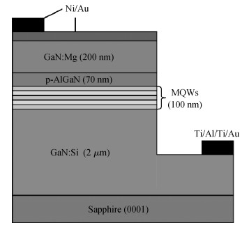
Processing math: 100%
J. Semicond. > 2014, Volume 35 > Issue 4 > 044007

SEMICONDUCTOR DEVICES

Electron-leakage-related low-temperature light emission efficiency behavior in GaN-based blue light-emitting diodes

Dawei Yan1, Lisha Li1, Jian Ren1, Fuxue Wang1, Guofeng Yang2, Shaoqing Xiao1 and Xiaofeng Gu1,

+ Author Affiliations

 Corresponding author: Gu Xiaofeng, Email: xgu@jiangnan.edu.cn

DOI: 10.1088/1674-4926/35/4/044007

PDF

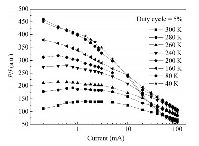
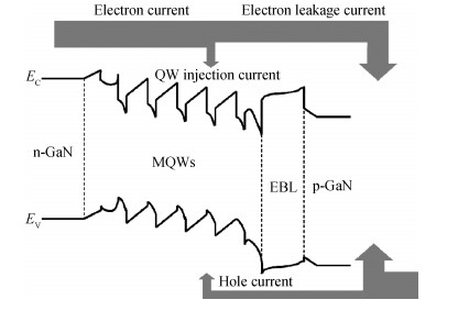
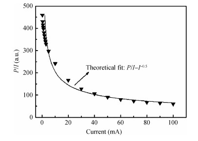
Abstract: The typical light emission efficiency behaviors of InGaN/GaN multi-quantum well (MQW) blue light-emitting diodes (LEDs) grown on c-plane sapphire substrates are characterized by pulsed current operation mode in the temperature range 40 to 300 K. At temperatures lower than 80 K, the emission efficiency of the LEDs decreases approximately as an inverse square root relationship with drive current. We use an electron leakage model to explain such efficiency droop behavior; that is, the excess electron leakage into the p-side of the LEDs under high forward bias will significantly reduce the injection possibility of holes into the active layer, which in turn leads to a rapid reduction in the radiative recombination efficiency in the MQWs. Combining the electron leakage model and the quasi-neutrality principle in the p-type region, we can readily derive the inverse square root dependent function between the light emission efficiency and the drive current. It appears that the excess electron leakage into the p-type side of the LEDs is primarily responsible for the low-temperature efficiency droop behavior.

Key words: gallium nitridelight-emitting diodeemission efficiencyelectron leakage

InGaN/GaN multi-quantum well (MQW) light-emitting diodes (LEDs) exhibit surprisingly high quantum efficiencies at room temperature (RT), despite the presence of a high density of threading dislocations in the films prepared by hetero-epitaxial growth, making them perfect candidates for general solid-state lighting applications[1]. Unfortunately, GaN-based LEDs normally only hit their peak efficiency at relatively low current densities ($\sim $10 A/cm$^{2})$ and suffer from an emerging efficiency reduction problem at higher injection levels: the so-called efficiency droop phenomenon. Negative efficiency droop occurs not only in blue LEDs, but also in green and ultraviolet devices, which severely deteriorates the performance of the diodes in critical high-current applications[2]. It is therefore essential to reveal the physical origin of this droop behavior. Many researchers from all over the world have performed intensive investigations into this critical issue, and several competing mechanisms have been proposed, including enhanced Auger recombination at high current densities, polarization field induced electron leakage, carrier delocalization from radiative recombination centers, and a shortage of holes due to inefficient ionization of the p-type dopant[3-7]. However, to date, none of these models has been generally accepted, and many confusing and sometimes contradictory observations and explanations of droop behavior still exist[8].

In this work, based on the fact that most of the structure and electronic defects in (In)GaN are generally optically deactivated at low temperatures, we present a study on the low-temperature light emission efficiency behaviors of the GaN-based blue LEDs[9]. We qualitatively explain the observed high-current efficiency reduction behavior, and theoretically derive the inverse square root dependence between the light emission efficiency and the drive current. We suggest that the excess electron leakage into the p-type side of the LEDs may be the major cause for the efficiency droop behavior.

The LED samples used in this study have an InGaN/GaN MQW structure grown on $c$-plane sapphire substrates using metal-organic chemical vapor deposition. Figure 1 shows the cross section of an InGaN/GaN MQW blue LED. The epistructure consists of a 2 $\mu $m GaN:Si n-contact layer ($N_{\rm D}$ $\approx$ --5 $\times $ 10$^{18}$ cm$^{-3})$, a ten-period of 3 nm undoped In$_{0.2}$Ga$_{0.8}$N and 7 nm GaN:Si MQW layer, a 70 nm p-AlGaN electron blocking layer (EBL), and a 0.2 $\mu $m GaN:Mg ($N_{\rm A}$ > 1 $\times $ 10$^{19}$ cm$^{-3})$ p-contact layer. LED chips with a mesa size of 300 $\times $ 300 $\mu $m$^{2}$ were fabricated using standard photolithography and dry etching processes. Annealed Ti/Al/Ti/Au and Ni/Au (2.5 nm/2.5 nm) multi-layers deposited by e-beam evaporation were employed as the ohmic contact and semi-transparent p-contact, respectively.

Figure  1.  Schematic cross section of an InGaN/GaN MQW blue LED grown on sapphire substrates.

The current-dependent emission intensity (proportional to the radiant flux) was measured under pulsed operation, with the injection current ranging from $\sim $10$^{-6}$ to 0.1 A. With this pulsed driving test, the self-heating effect in the LEDs can be substantially suppressed. The peak emission wavelength of the LEDs is about 466 nm with a full-width-at-half-maximum of 36 nm. The emission efficiency is approximately denoted by the ratio of EL intensity $P$ to current $I$ in this work.

Figure 2 shows the experimental light emission efficiencies as a function of drive current measured at different temperatures. At low temperatures, the emission efficiency of the LEDs displays a monotonous decrease with current, while with a further increase in temperature, the efficiency curve exhibits a typical roll-off behavior, with a maximum value at $\sim $10 A/cm$^{2}$. Low emission efficiency on the low-current side of the maxima can be due to enhanced nonradiative recombination at the extended crystal defects in the active layer. Its dependence on current (and thus carrier density) can be described by the Shockley--Read--Hall model $\sim Bn^{2}$/$(Bn^{2}+An)$, where $Bn^{2}$ and $An$ are the radiative and nonradiative recombination rates, respectively, and $n$ is the free carrier concentration[10]. With increasing injection current, the emission efficiency of the LEDs is expected to quickly approach unity[11]. The movement of the current at the efficiency maxima towards the high-current direction at elevated temperatures can be attributed to the increased concentration of positively charged holes in the p-side of the LEDs[6]. The droop origin on the high-current side of the efficiency maxima has been a controversial subject. In the following, based on the idea that most of the structure and electronic defects in â…¢-nitride materials are generally optically deactivated at low temperatures, we study the low-temperature efficiency reduction behavior of the LEDs.

Figure  2.  Emission efficiency ($P/I$) as a function of drive current measured at various temperatures. The drive current ($x$-axis) is plotted in a semi-log scale. Typical efficiency droop behavior was observed at $T$ > 200 K.

We consider first the forward current transport characteristics of the GaN-based LEDs, since the major recombination processes of the electron--hole pairs are closely associated with these charge injection processes. Figure 3 shows the $I$--$V$ curves measured at 60, 80 and 100 K, respectively. As can be seen, these curves have identical bias dependences but are almost insensitive to temperature, which indicates that the current is mainly due to tunneling rather than a recombination process. An empirical equation for an experimental $I$--$V$ relationship of a pn junction is usually given by

$ JFexpqVnkT,

$

(1)
Figure  3.  The typical $I$--$V$ curves of the LEDs measured below 100 K. The extracted ideality factors at 80 K in the low-and medium-bias regions are 19.5 and 7.5, respectively, indicating the dominant tunneling mechanism. In the bias region (c), the current transport is influenced by a bulk resistance effect.

where the ideality factor $n$ $=$ 2 when the recombination current dominates and $n$ $=$ 1 when the diffusion current dominates. However, when the tunneling current is significant, $n$ has a value much larger than 2. Depending on the bias level, two successive linearly dependent segments with different slopes can be observed in the low-and medium-bias regions. The corresponding ideality factors determined from the current slopes are 19.5 and 7.5 at 100 K, respectively. According to our previous work, the current in the low-bias region (segment a) might be dominated by electron tunneling through defect-induced intermediate states, while in the medium-bias region (segment b), the heavy holes can be the dominant tunneling entities[12]. At higher current levels ($>$ 0.1 mA), the $I$--$V$ curves gradually bend downwards, which is caused by an increasing voltage drop on the series resistance of the diodes. Visible light emission can be detected even at temperatures as low as 10 K (not shown here), indicating that a complete carrier freeze-out does not occur in the diodes. Since the ionization energy of the p-type dopant: Mg ($\sim $150--200 meV) is considerably larger than that of the n-type dopant: Si ($\sim $20 meV) in GaN, the electrons are the excess carriers and the holes are the minority. Therefore, under high forward bias, where the conduction band on the n-side becomes relatively higher than the conduction band on the p-side, many electrons can have sufficient kinetic energy to fly over the quantum well and the EBL barriers into the p-side of the LEDs[13].

Figure 4 schematically illustrates the individual current component inside the LEDs under the high forward-bias condition. From the illustration, we can readily deduced that, (1) an increase in drive bias will cause a greater fraction of electrons to escape from the MQW region into the p-side of the LEDs, where they will recombine non-radiatively with the holes, and (2) the radiative recombination current within the MQW layer equals the hole current $I_{\rm hole}$ injected from the p-side into the active layer. At high forward bias, $I_{\rm hole}$ is not as important as electron leakage current $I_{\rm Leak}$, and the emission efficiency of the LEDs can be represented by

$ η=IholeILeak,

$

(2)
Figure  4.  Schematic illustration of the current components in the LEDs at high drive biases.

where $I_{\rm Leak}$ is the electron leakage current component. In addition, the relationship between $I_{\rm hole}$ and $I_{\rm Leak}$ can be empirically approximated by

$ ILeak=CIKQW,

$

(3)

where both $C$ and $K$ are the fitting parameters[14]. It is believed that Equation (3) not only covers the carrier leakage by TE from the quantum wells, but can also be used for the fly-over carriers not captured by the quantum wells, or for the trap-assisted tunneling leakage[15]. Then, substituting Eq. (3) into Eq. (2), yields

$ η=αImLeak,

$

(4)
Figure  5.  The dependence of the LED emission efficiency on the drive current at 80 K. The solid line is the theoretical fitting result with $m$ $=$ $-$0.5.

where $\alpha =C^{-1/K}$, $m=1/K$ --1. This equation predicts that at a given low temperature, the emission efficiency and the electron leakage current of the LEDs should follow a power-law dependent relationship. Figure 4 shows the experimental result measured at 80 K. As observed, these data points can be nicely fitted with $m=$ $-0.5$ in the measured drive current range, which is consistent with the form of Eq. (4).

We shall now briefly address the low-temperature efficiency curve with $m =$ $-$0.5. The generation rate of minority carriers is extremely slow due to the wide bandgap nature of GaN, so the generation process may be discarded in the analysis. With low temperature and high forward bias conditions, the electron leakage current into the p-type region of the LEDs should approximately equal the recombination current $I_{\rm R}$ in the p-type side:

$ ILeak=IRRneph,

$

(5)

where $R$ is the non-radiative recombination coefficient, $n_{\rm e}$ the concentration of electrons captured by the various traps and acceptors, and $p_{\rm h}$ the concentration of holes induced by the injected electrons. To satisfy the electro-neutrality condition in the p-type region, we have

$ phne.

$

(6)

Substituting Eq. (6) into Eq. (5) yields

$ ILeakp2h.

$

(7)

At high injection levels

$ IPphILeakI,

$

(8)

and combining with Eq. (7) gives

$ PII0.5.

$

(9)

Obviously, Equation (9) predicts an inverse square root dependent relationship between the emission efficiency and the drive current, which is in good agreement with the experimental result. This consistency supports the light emission efficiency droop behavior of the GaN-based LEDs at low-temperature being well explained by the electron leakage model, and electron leakage might be the essential cause of a significant efficiency reduction at high current levels.

Finally, it is worth noting that although the strong polarization field can effectively reduce the barrier to electron leakage from the quantum well and over the EBL, and Auger recombination can produce high-energy electrons far above the EBL conduction band-edge, enhancing the electron leakage behavior of the LEDs, neither of them can be the major cause of efficiency droop because obvious efficiency collapse behavior has been detected in the nonpolar $m$-plane samples and at extremely low current density (Auger recombination becomes significant only at high carrier densities), respectively. Furthermore, there is no obvious improvement in the droop performance of the LEDs on bulk GaN substrates, with the low-density defects not greatly improved compared with those of conventional $c$-plane chips, indicating that the carrier delocalization regime may not be the main cause of the droop either[16].

The emission efficiency of GaN-based blue LEDs was measured and studied. The low-temperature efficiency curves show an inverse square root dependent relationship as a function of drive current. The forward-bias current characteristics suggest that the large electron injection into the p-side of the LEDs can suppress the effective injection of holes into the quantum wells, resulting in decreased emission efficiency. Based on the electron leakage model, the inverse square root dependent relationship between the emission efficiency and drive current is derived, and is in good agreement with the experimental observation. Electron leakage may be the real cause of efficiency droop in LEDs at low temperature.


[1]
Lester S D, Ponce F A, Graford M G, et al. High dislocation densities in high efficiency GaN-based light-emitting diodes. Appl Phys Lett, 1995, 66:1249 doi: 10.1063/1.113252
[2]
Yang Y, Cao X A, Yan C. Investigation of the nonthermal mechanism of efficiency rolloff in InGaN light-emitting diodes. IEEE Trans Electron Devices, 2008, 55:1771 doi: 10.1109/TED.2008.923561
[3]
Iveland J, Martinelli L, Peretti J, et al. Direct measurement of auger electrons emitted from a semiconductor light-emitting diode under electrical injection:identification of the dominant mechanism for efficiency droop. Phys Rev Lett, 2013, 110:177406 doi: 10.1103/PhysRevLett.110.177406
[4]
Kim M H, Schubert M F, Dai Q, et al. Origin of efficiency droop in GaN-based light-emitting diodes. Appl Phys Lett, 2007, 91:183507 doi: 10.1063/1.2800290
[5]
Mukai T, Yamada M, Nakamura S J. Characteristics of InGaN-based UV/blue/green/amber/red light-emitting diodes. Jpn J Appl Phys Part 1, 1999, 38:3976 doi: 10.1143/JJAP.38.3976
[6]
Masui H, Kroemer H, Schmidt M C, et al. Electroluminescence efficiency of-oriented InGaN-based light-emitting diodes at low temperature. J Phys D:Appl Phys, 2008, 41:0822001 http://cat.inist.fr/?aModele=afficheN&cpsidt=20270880
[7]
Choi S, Ji M H, Kim J, et al. Efficiency droop due to electron spill-over and limited hole injection in Ⅲ-nitride visible light-emitting diodes employing lattice-matched InAlN electron blocking layers. Appl Phys Lett, 2012, 101:161110 doi: 10.1063/1.4759044
[8]
Bertazzi F, Goano M, Bellotti E. Numerical analysis of indirect Auger transitions in InGaN. Appl Phys Lett, 2012, 101:011111 doi: 10.1063/1.4733353
[9]
Cao X A, Stokes E B, Sandvik P M, et al. Diffusion and tunneling currents in GaN/InGaN multiple quantum well light-emitting diodes. IEEE Electron Device Lett, 2002, 23:535 doi: 10.1109/LED.2002.802601
[10]
Piprek J. Semiconductor optoelectronic devices:introduction to physics and simulation. Academic Press, 2007
[11]
Shao X J, Lu H, Chen D J, et al. Efficiency droop behavior of GaN-based light emitting diodes under reverse-current and high-temperature stress. Appl Phys Lett, 2009, 95:163504 doi: 10.1063/1.3254237
[12]
Yan D W, Lu H, Chen D J, et al. Forward tunneling current in GaN-based blue light-emitting diodes. Appl Phys Lett, 2010, 96:083504 doi: 10.1063/1.3327332
[13]
Masui H, Sato H, Asamizu H, et al. Radiative recombination efficiency of InGaN-Based light-emitting diodes evaluated at various temperatures and injection currents. Jpn J Appl Phys, 2007, 46:L627 http://stacks.iop.org/1347-4065/46/L627
[14]
Piprek J. Efficiency droop in nitride-based light-emitting diodes. Phys Status Solid A, 2010, 207:2217 doi: 10.1002/pssa.v207:10
[15]
Yang Y, Cao X A, Yan C H. Rapid efficiency roll-off in high-quality green light-emitting diodes on freestanding GaN substrates. Appl Phys Lett, 2009, 94:041117 doi: 10.1063/1.3077017
[16]
Schubert M F, Chhajed S, Kim J K, et al. Effect of dislocation density on efficiency droop in GalnN/GaN light-emitting diodes. Appl Phys Lett, 2007, 91:231114 doi: 10.1063/1.2822442
Fig. 1.  Schematic cross section of an InGaN/GaN MQW blue LED grown on sapphire substrates.

Fig. 2.  Emission efficiency ($P/I$) as a function of drive current measured at various temperatures. The drive current ($x$-axis) is plotted in a semi-log scale. Typical efficiency droop behavior was observed at $T$ > 200 K.

Fig. 3.  The typical $I$--$V$ curves of the LEDs measured below 100 K. The extracted ideality factors at 80 K in the low-and medium-bias regions are 19.5 and 7.5, respectively, indicating the dominant tunneling mechanism. In the bias region (c), the current transport is influenced by a bulk resistance effect.

Fig. 4.  Schematic illustration of the current components in the LEDs at high drive biases.

Fig. 5.  The dependence of the LED emission efficiency on the drive current at 80 K. The solid line is the theoretical fitting result with $m$ $=$ $-$0.5.

[1]
Lester S D, Ponce F A, Graford M G, et al. High dislocation densities in high efficiency GaN-based light-emitting diodes. Appl Phys Lett, 1995, 66:1249 doi: 10.1063/1.113252
[2]
Yang Y, Cao X A, Yan C. Investigation of the nonthermal mechanism of efficiency rolloff in InGaN light-emitting diodes. IEEE Trans Electron Devices, 2008, 55:1771 doi: 10.1109/TED.2008.923561
[3]
Iveland J, Martinelli L, Peretti J, et al. Direct measurement of auger electrons emitted from a semiconductor light-emitting diode under electrical injection:identification of the dominant mechanism for efficiency droop. Phys Rev Lett, 2013, 110:177406 doi: 10.1103/PhysRevLett.110.177406
[4]
Kim M H, Schubert M F, Dai Q, et al. Origin of efficiency droop in GaN-based light-emitting diodes. Appl Phys Lett, 2007, 91:183507 doi: 10.1063/1.2800290
[5]
Mukai T, Yamada M, Nakamura S J. Characteristics of InGaN-based UV/blue/green/amber/red light-emitting diodes. Jpn J Appl Phys Part 1, 1999, 38:3976 doi: 10.1143/JJAP.38.3976
[6]
Masui H, Kroemer H, Schmidt M C, et al. Electroluminescence efficiency of-oriented InGaN-based light-emitting diodes at low temperature. J Phys D:Appl Phys, 2008, 41:0822001 http://cat.inist.fr/?aModele=afficheN&cpsidt=20270880
[7]
Choi S, Ji M H, Kim J, et al. Efficiency droop due to electron spill-over and limited hole injection in Ⅲ-nitride visible light-emitting diodes employing lattice-matched InAlN electron blocking layers. Appl Phys Lett, 2012, 101:161110 doi: 10.1063/1.4759044
[8]
Bertazzi F, Goano M, Bellotti E. Numerical analysis of indirect Auger transitions in InGaN. Appl Phys Lett, 2012, 101:011111 doi: 10.1063/1.4733353
[9]
Cao X A, Stokes E B, Sandvik P M, et al. Diffusion and tunneling currents in GaN/InGaN multiple quantum well light-emitting diodes. IEEE Electron Device Lett, 2002, 23:535 doi: 10.1109/LED.2002.802601
[10]
Piprek J. Semiconductor optoelectronic devices:introduction to physics and simulation. Academic Press, 2007
[11]
Shao X J, Lu H, Chen D J, et al. Efficiency droop behavior of GaN-based light emitting diodes under reverse-current and high-temperature stress. Appl Phys Lett, 2009, 95:163504 doi: 10.1063/1.3254237
[12]
Yan D W, Lu H, Chen D J, et al. Forward tunneling current in GaN-based blue light-emitting diodes. Appl Phys Lett, 2010, 96:083504 doi: 10.1063/1.3327332
[13]
Masui H, Sato H, Asamizu H, et al. Radiative recombination efficiency of InGaN-Based light-emitting diodes evaluated at various temperatures and injection currents. Jpn J Appl Phys, 2007, 46:L627 http://stacks.iop.org/1347-4065/46/L627
[14]
Piprek J. Efficiency droop in nitride-based light-emitting diodes. Phys Status Solid A, 2010, 207:2217 doi: 10.1002/pssa.v207:10
[15]
Yang Y, Cao X A, Yan C H. Rapid efficiency roll-off in high-quality green light-emitting diodes on freestanding GaN substrates. Appl Phys Lett, 2009, 94:041117 doi: 10.1063/1.3077017
[16]
Schubert M F, Chhajed S, Kim J K, et al. Effect of dislocation density on efficiency droop in GalnN/GaN light-emitting diodes. Appl Phys Lett, 2007, 91:231114 doi: 10.1063/1.2822442
1

Hydride vapor phase epitaxy for gallium nitride substrate

Jun Hu, Hongyuan Wei, Shaoyan Yang, Chengming Li, Huijie Li, et al.

Journal of Semiconductors, 2019, 40(10): 101801. doi: 10.1088/1674-4926/40/10/101801

2

Rational molecular passivation for high-performance perovskite light-emitting diodes

Jingbi You

Journal of Semiconductors, 2019, 40(4): 040203. doi: 10.1088/1674-4926/40/4/040203

3

Light-emitting diodes based on colloidal silicon quantum dots

Shuangyi Zhao, Xiangkai Liu, Xiaodong Pi, Deren Yang

Journal of Semiconductors, 2018, 39(6): 061008. doi: 10.1088/1674-4926/39/6/061008

4

Suppression of electron leakage in 808 nm laser diodes with asymmetric waveguide layer

Xiang Li, Degang Zhao, Desheng Jiang, Ping Chen, Zongshun Liu, et al.

Journal of Semiconductors, 2016, 37(1): 014007. doi: 10.1088/1674-4926/37/1/014007

5

Progress in complementary metal-oxide-semiconductor silicon photonics and optoelectronic integrated circuits

Hongda Chen, Zan Zhang, Beiju Huang, Luhong Mao, Zanyun Zhang, et al.

Journal of Semiconductors, 2015, 36(12): 121001. doi: 10.1088/1674-4926/36/12/121001

6

Influences of ICP etching damages on the electronic properties of metal field plate 4H-SiC Schottky diodes

Hui Wang, Yingxi Niu, Fei Yang, Yong Cai, Zehong Zhang, et al.

Journal of Semiconductors, 2015, 36(10): 104006. doi: 10.1088/1674-4926/36/10/104006

7

The effects of electron irradiation on the optical properties of the organic semiconductor polypyrrole

J. V. Thombare, M. C. Rath, S. H. Han, V. J. Fulari

Journal of Semiconductors, 2013, 34(9): 093001. doi: 10.1088/1674-4926/34/9/093001

8

Thermal simulation and analysis of flat surface flip-chip high power light-emitting diodes

Maoxing Chen, Chen Xu, Kun Xu, Lei Zheng

Journal of Semiconductors, 2013, 34(12): 124005. doi: 10.1088/1674-4926/34/12/124005

9

AC-electronic and dielectric properties of semiconducting phthalocyanine compounds:a comparative study

Safa'a M. Hraibat, Rushdi M-L. Kitaneh, Mohammad M. Abu-Samreh, Abdelkarim M. Saleh

Journal of Semiconductors, 2013, 34(11): 112001. doi: 10.1088/1674-4926/34/11/112001

10

Electrical characterization of the organic semiconductor Ag/CuPc/Au Schottky diode

Mutabar Shah, M. H. Sayyad, Kh. S. Karimov

Journal of Semiconductors, 2011, 32(4): 044001. doi: 10.1088/1674-4926/32/4/044001

11

Degradation of light emitting diodes: a proposed methodology

Sau Koh, Willem Van Driel, G. Q. Zhang

Journal of Semiconductors, 2011, 32(1): 014004. doi: 10.1088/1674-4926/32/1/014004

12

Fluorescent SiC and its application to white light-emitting diodes

Satoshi Kamiyama, Motoaki Iwaya, Tetsuya Takeuchi, Isamu Akasaki, Mikael Syvajarvi, et al.

Journal of Semiconductors, 2011, 32(1): 013004. doi: 10.1088/1674-4926/32/1/013004

13

Properties of the ITO layer in a novel red light-emitting diode

Zhang Yonghui, Guo Weiling, Gao Wei, Li Chunwei, Ding Tianping, et al.

Journal of Semiconductors, 2010, 31(4): 043002. doi: 10.1088/1674-4926/31/4/043002

14

Room-temperature electroluminescence of p-ZnxMg1-xO:Na/n-ZnO p-n junction light emitting diode

Ye Zhizhen, Zhang Liqiang, Huang Jingyun, Zhang Yinzhu, Zhu Liping, et al.

Journal of Semiconductors, 2009, 30(8): 081001. doi: 10.1088/1674-4926/30/8/081001

15

Spectrum study of top-emitting organic light-emitting devices with micro-cavity structure

Liu Xiang, Wei Fuxiang, Liu Hui

Journal of Semiconductors, 2009, 30(4): 044007. doi: 10.1088/1674-4926/30/4/044007

16

Thermal Simulation and Analysis of High Power Flip-Chip Light-Emitting Diode System

Wang Libin, Liu Zhiqiang, Chen Yu, Yi Xiaoyan, Ma Long, et al.

Chinese Journal of Semiconductors , 2007, 28(S1): 504-508.

17

Influence of an Omni-Directional Reflector on the Luminous Efficiency of AlGaInP Light-Emitting Diodes

Sun Hao, Han Jun, Li Jianjun, Deng Jun, Zou Deshu, et al.

Chinese Journal of Semiconductors , 2007, 28(12): 1952-1956.

18

Electronic Structure of Semiconductor Nanocrystals

Li Jingbo, Wang Linwang, Wei Suhuai

Chinese Journal of Semiconductors , 2006, 27(2): 191-196.

19

A High Performance Sub-100nm Nitride/Oxynitride Stack Gate Dielectric CMOS Device with Refractory W/TiN Metal Gates

Zhong Xinghua, Zhou Huajie, Lin Gang, Xu Qiuxia

Chinese Journal of Semiconductors , 2006, 27(3): 448-453.

20

Fabrication and Emission Properties of a n-ZnO/p-GaN Heterojunction Light-Emitting Diode

Zhou Xin, Gu Shulin, Zhu Shunming, Ye Jiandong, Liu Wei, et al.

Chinese Journal of Semiconductors , 2006, 27(2): 249-253.

  • Search

    Advanced Search >>

    GET CITATION

    Dawei Yan, Lisha Li, Jian Ren, Fuxue Wang, Guofeng Yang, Shaoqing Xiao, Xiaofeng Gu. Electron-leakage-related low-temperature light emission efficiency behavior in GaN-based blue light-emitting diodes[J]. Journal of Semiconductors, 2014, 35(4): 044007. doi: 10.1088/1674-4926/35/4/044007
    D W Yan, L S Li, J Ren, F X Wang, G F Yang, S Q Xiao, X F Gu. Electron-leakage-related low-temperature light emission efficiency behavior in GaN-based blue light-emitting diodes[J]. J. Semicond., 2014, 35(4): 044007. doi: 10.1088/1674-4926/35/4/044007.
    shu

    Export: BibTex EndNote

    Article Metrics

    Article views: 2432 Times PDF downloads: 15 Times Cited by: 0 Times

    History

    Received: 21 September 2013 Revised: 20 November 2013 Online: Published: 01 April 2014

    Catalog

      Email This Article

      User name:
      Email:*请输入正确邮箱
      Code:*验证码错误
      Dawei Yan, Lisha Li, Jian Ren, Fuxue Wang, Guofeng Yang, Shaoqing Xiao, Xiaofeng Gu. Electron-leakage-related low-temperature light emission efficiency behavior in GaN-based blue light-emitting diodes[J]. Journal of Semiconductors, 2014, 35(4): 044007. doi: 10.1088/1674-4926/35/4/044007 ****D W Yan, L S Li, J Ren, F X Wang, G F Yang, S Q Xiao, X F Gu. Electron-leakage-related low-temperature light emission efficiency behavior in GaN-based blue light-emitting diodes[J]. J. Semicond., 2014, 35(4): 044007. doi: 10.1088/1674-4926/35/4/044007.
      Citation:
      Dawei Yan, Lisha Li, Jian Ren, Fuxue Wang, Guofeng Yang, Shaoqing Xiao, Xiaofeng Gu. Electron-leakage-related low-temperature light emission efficiency behavior in GaN-based blue light-emitting diodes[J]. Journal of Semiconductors, 2014, 35(4): 044007. doi: 10.1088/1674-4926/35/4/044007 ****
      D W Yan, L S Li, J Ren, F X Wang, G F Yang, S Q Xiao, X F Gu. Electron-leakage-related low-temperature light emission efficiency behavior in GaN-based blue light-emitting diodes[J]. J. Semicond., 2014, 35(4): 044007. doi: 10.1088/1674-4926/35/4/044007.

      Electron-leakage-related low-temperature light emission efficiency behavior in GaN-based blue light-emitting diodes

      DOI: 10.1088/1674-4926/35/4/044007
      Funds:

      the National Natural Science Foundation of China 11074280

      the Natural Science Foundation of Jiangsu Province, China BK2012110

      the State Key Laboratory of ASIC and System 11KF003

      the Chinese Postdoctoral Science Foundation 2013M540437

      Project supported by the National Natural Science Foundation of China (No. 11074280), the Natural Science Foundation of Jiangsu Province, China (No. BK2012110), the Fundamental Research Funds for the Central Universities of China (No. JUSRP51323B), the Chinese Postdoctoral Science Foundation (No. 2013M540437), the State Key Laboratory of ASIC and System (No. 11KF003), and the PAPD of Jiangsu Higher Education Institutions and the Summit of the Six Top Talents Program of Jiangsu Province (No. DZXX-053)

      the PAPD of Jiangsu Higher Education Institutions and the Summit of the Six Top Talents Program of Jiangsu Province DZXX-053

      More Information
      • Corresponding author: Gu Xiaofeng, Email: xgu@jiangnan.edu.cn
      • Received Date: 2013-09-21
      • Revised Date: 2013-11-20
      • Published Date: 2014-04-01

      Catalog

        /

        DownLoad:  Full-Size Img  PowerPoint
        Return
        Return