Fig. 1.
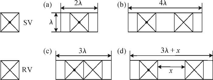
The occupied area of routing patterns. (a) SV. (b) DV. (c) REV. (d) LLV.
SEMICONDUCTOR INTEGRATED CIRCUITS
Junping Wang1, 2, , Dan Xu1 and Yongbang Su2
Corresponding author: Wang Junping, Email:jpwang@mail.xidian.edu.cn
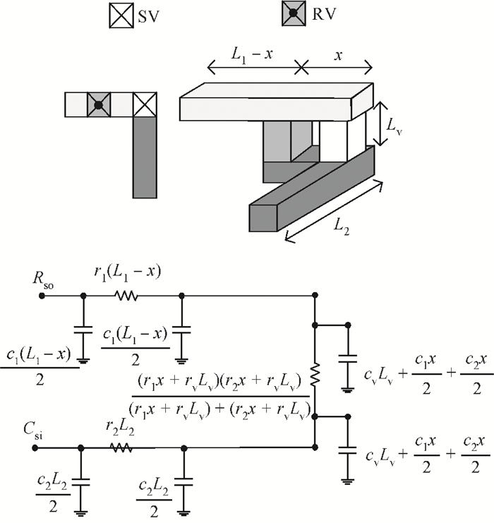
Abstract: Redundant via (RV) insertion is a useful mechanism to enhance via reliability. However, when extra vias are inserted into the design, the circuit timing might be changed. Therefore, how to insert RV under the timing constraints is the main challenge. In this paper, we introduce a new model to compute the distance between a RV and the corresponding single via, put forward a new RV type, which is called the long length via (LLV), and then present an improved RV insertion method considering the timing constraints. This computing model can certify that the timing, which is obtained after inserting a RV, is not greater than the original timing. Meanwhile, the new RV type LLV can increase the possibility of RV insertion; this method provides a global perspective for the RV insertion. Considering the timing constraints, the total redundant via insertion rate is 85.38% in the MIS-based method, while our proposed method can obtain a high insertion rate 88.79% for the tested circuits.
Keywords: redundant via, timing constraints, integrated circuit
| [1] |
Chen Wenbiao, Chen Lan, Li Zhigang, et al. Effects of pattern characteristics on the copper electroplating process. Journal of Semiconductors, 2011, 32(5):055010 doi: 10.1088/1674-4926/32/5/055010
|
| [2] |
Yang Yiwei, Shi Zheng, Yan Xiaolang. Model-based dynamic dissection in OPC. Journal of Semiconductors, 2008, 29(7):1422 http://www.jos.ac.cn/bdtxbcn/ch/reader/view_abstract.aspx?file_no=07110903&flag=1
|
| [3] |
Liang Tao, Jia Xinzhang. A numerical integration-based yield estimation method for integrated circuits. Journal of Semiconductors, 2011, 32(4):045012 doi: 10.1088/1674-4926/32/4/045012
|
| [4] |
Wang Junping, Hao Yue. Yield modeling of rectangular defect outline. Chinese Journal of Semiconductors, 2005, 26(8):1514 http://www.oalib.com/paper/1518454
|
| [5] |
Liang Tao, Jia Xinzhang. An empirical formula for yield estimation from singly truncated performance data of qualified semiconductor devices. Journal of Semiconductors, 2012, 33(12):125008 doi: 10.1088/1674-4926/33/12/125008
|
| [6] |
Yang Yintang, Leng Peng, Dong Gang, et al. RLC interconnect delay with temperature distribution effects. Journal of Semiconductors, 2008, 29(9):1843 http://www.jos.ac.cn/bdtxbcn/ch/reader/view_abstract.aspx?file_no=07112202&flag=1
|
| [7] |
Li X, Wang J M, Tang W, et al. Stochastic analysis of interconnect delay in the presence of process variations. Journal of Semiconductors, 2008, 29(2):304 http://www.jos.ac.cn/bdtxbcn/ch/reader/view_abstract.aspx?file_no=07082201&flag=1
|
| [8] |
Barnt T S, Bickford J, Weger A J. Product yield prediction system and critical area database. IEEE Trans Semicond Manufac, 2007, 21(3):351 http://ieeexplore.ieee.org/document/4589022/
|
| [9] |
Ducotey G, Couvrat A, Audran V. In-line methodology for defectivity analysis form dark field wafer inspection to defect root cause analysis using FIB cut. Advanced Semiconductor Manufacturing Conference, 2008 http://ieeexplore.ieee.org/document/4529041/?reload=true&arnumber=4529041&punumber%3D4519622
|
| [10] |
Izuka T, IkedaM, Asada K. Timing-aware cell layout de-compaction for yield optimization by critical area minimization. IEEE Trans VLSI Syst, 2007, 15(6):716 doi: 10.1109/TVLSI.2007.898754
|
| [11] |
Wang J P, Hao Y. Critical area computation for real defects and arbitary conductor shapes. Acta Electronica Sinica, 2006, 34(4):1974 http://cpb.iphy.ac.cn/EN/Y2006/V15/I7/1621
|
| [12] |
Beanato G, Giovannini P, Cevrero A. Design and testing strategies for modular 3-D-multiprocessor systems using die-level through silicon via technology. IEEE J Emerging and Selected Topics in Circuits and Systems, 2012, 2(2):295 doi: 10.1109/JETCAS.2012.2193837
|
| [13] |
Ting F C, Tsang C K, Shih H Y. Enhanced redundant via insertion with multi-via mechanisms. IEEE Computer Society Annual Symposium on VLSI, 2011 http://ieeexplore.ieee.org/document/5992483/
|
| [14] |
Xu G, Huang L D, Pan D Z. Redundant-via enhanced maze routing for yield improvement. Proceedings of the ASP-DAC, 2005 http://dl.acm.org/citation.cfm?id=1120927
|
| [15] |
Lee K Y, Koh C K, Wang T C. Fast and optimal redundant via insertion. IEEE Trans Computer-Aided Design of Integrated Circuits and Systems, 2008, 27(12):2194 http://ieeexplore.ieee.org/document/4670066/
|
| [16] |
Chen H Y, Chiang M F, Chang Y W. Full-chip routing considering double-via insertion. IEEE Trans Computer-Aided Design of Integrated Circuits and Systems, 2010, 27(5):844 http://dl.acm.org/citation.cfm?id=2301984
|
| [17] |
Chang T F, Kan T C, Yang S H. Enhanced redundant via insertion with multi-via mechanisms. The 14th IEEE Computer Society Annual Symposium on VLSI, 2011 http://ieeexplore.ieee.org/document/5992483/
|
| [18] |
Kan T C K, Yang S H, Chang T F. Design of a practical nanometer-scale redundant via-aware standard cell library for improved redundant via1 insertion rate. IEEE Trans VLSI Syst, 2013, 21(1):142 doi: 10.1109/TVLSI.2011.2176968
|
| [19] |
Yao H L, Cai Y, Zhou Q. Multilevel routing with redundant via insertion. IEEE Trans Circuits Syst, 2006, 53(10):1148 doi: 10.1109/TCSII.2006.881822
|
| [20] |
Allan G A. Targeted layout modifications for semiconductor yield/reliability enhancement. IEEE Trans Semicond Manufacturing, 2004, 17(4):573 doi: 10.1109/TSM.2004.835727
|
| [21] |
Hao Ran, Wang Huijuan, Yu Daquan, et al. High-speed through-silicon via filling method using Cu-cored solder balls. Journal of Semiconductors, 2012, 33(8):086002 doi: 10.1088/1674-4926/33/8/086002
|
| [22] |
Haltmeier M. Stable signal reconstruction via minimization in redundant, non-tight frames. IEEE Trans Signal Processing, 2013, 61(2):420 doi: 10.1109/TSP.2012.2222396
|
| [23] |
Shen J W, Chiang M F, Chen S. Redundant via allocation for layer partition-based redundant via insertion. IEEE 8th International Conference on ASIC, 2009 http://ieeexplore.ieee.org/document/5351310/
|
| [24] |
Liang J, Chen S, Yoshimura T. Redundant via insertion based on conflict removal. ICSICT, 2010 http://ieeexplore.ieee.org/xpls/abs_all.jsp?arnumber=5667425
|
| [25] |
Luo F, Jia Y, Dai W M. Yield-preferred via insertion based on novel geotopological technology. Asia and South Pacific Conference on Design Automation, 2006 http://dl.acm.org/citation.cfm?id=1118469
|
| [26] |
Pan C W, Lee Y M. Redundant via insertion under timing constraints. The 12th International Symposium on Quality Electronic Design, 2011 http://ieeexplore.ieee.org/xpls/icp.jsp?arnumber=5770794
|
| [27] |
Yan J T T, Chen Z W, Chiang B Y. Timing-constrained yield-driven redundant via insertion. APPCCAS, 2008 http://ieeexplore.ieee.org/xpls/abs_all.jsp?arnumber=4746363
|
| [28] |
Yan J T, Chiang B Y, Chen Z W. Yield-driven redundant via insertion based on probalilistic via-insertion analysis. International Conference on Electronics, Circuits and Systems, 2006 http://ieeexplore.ieee.org/xpls/abs_all.jsp?arnumber=4263506
|
| [29] |
Hao Y. Theory and methods of integrated circuits manufacturing dynamics. Beijing:Beijing Educational Press, 1995:132
|
Table 1. Test circuit information.

|
Table 2. RV insertion under no constraint with our method.

|
Table 3. RV insertion under timing constraint with our method.

|
Table 4. RV insertion under timing constraint in Ref. [26].

|
| [1] |
Chen Wenbiao, Chen Lan, Li Zhigang, et al. Effects of pattern characteristics on the copper electroplating process. Journal of Semiconductors, 2011, 32(5):055010 doi: 10.1088/1674-4926/32/5/055010
|
| [2] |
Yang Yiwei, Shi Zheng, Yan Xiaolang. Model-based dynamic dissection in OPC. Journal of Semiconductors, 2008, 29(7):1422 http://www.jos.ac.cn/bdtxbcn/ch/reader/view_abstract.aspx?file_no=07110903&flag=1
|
| [3] |
Liang Tao, Jia Xinzhang. A numerical integration-based yield estimation method for integrated circuits. Journal of Semiconductors, 2011, 32(4):045012 doi: 10.1088/1674-4926/32/4/045012
|
| [4] |
Wang Junping, Hao Yue. Yield modeling of rectangular defect outline. Chinese Journal of Semiconductors, 2005, 26(8):1514 http://www.oalib.com/paper/1518454
|
| [5] |
Liang Tao, Jia Xinzhang. An empirical formula for yield estimation from singly truncated performance data of qualified semiconductor devices. Journal of Semiconductors, 2012, 33(12):125008 doi: 10.1088/1674-4926/33/12/125008
|
| [6] |
Yang Yintang, Leng Peng, Dong Gang, et al. RLC interconnect delay with temperature distribution effects. Journal of Semiconductors, 2008, 29(9):1843 http://www.jos.ac.cn/bdtxbcn/ch/reader/view_abstract.aspx?file_no=07112202&flag=1
|
| [7] |
Li X, Wang J M, Tang W, et al. Stochastic analysis of interconnect delay in the presence of process variations. Journal of Semiconductors, 2008, 29(2):304 http://www.jos.ac.cn/bdtxbcn/ch/reader/view_abstract.aspx?file_no=07082201&flag=1
|
| [8] |
Barnt T S, Bickford J, Weger A J. Product yield prediction system and critical area database. IEEE Trans Semicond Manufac, 2007, 21(3):351 http://ieeexplore.ieee.org/document/4589022/
|
| [9] |
Ducotey G, Couvrat A, Audran V. In-line methodology for defectivity analysis form dark field wafer inspection to defect root cause analysis using FIB cut. Advanced Semiconductor Manufacturing Conference, 2008 http://ieeexplore.ieee.org/document/4529041/?reload=true&arnumber=4529041&punumber%3D4519622
|
| [10] |
Izuka T, IkedaM, Asada K. Timing-aware cell layout de-compaction for yield optimization by critical area minimization. IEEE Trans VLSI Syst, 2007, 15(6):716 doi: 10.1109/TVLSI.2007.898754
|
| [11] |
Wang J P, Hao Y. Critical area computation for real defects and arbitary conductor shapes. Acta Electronica Sinica, 2006, 34(4):1974 http://cpb.iphy.ac.cn/EN/Y2006/V15/I7/1621
|
| [12] |
Beanato G, Giovannini P, Cevrero A. Design and testing strategies for modular 3-D-multiprocessor systems using die-level through silicon via technology. IEEE J Emerging and Selected Topics in Circuits and Systems, 2012, 2(2):295 doi: 10.1109/JETCAS.2012.2193837
|
| [13] |
Ting F C, Tsang C K, Shih H Y. Enhanced redundant via insertion with multi-via mechanisms. IEEE Computer Society Annual Symposium on VLSI, 2011 http://ieeexplore.ieee.org/document/5992483/
|
| [14] |
Xu G, Huang L D, Pan D Z. Redundant-via enhanced maze routing for yield improvement. Proceedings of the ASP-DAC, 2005 http://dl.acm.org/citation.cfm?id=1120927
|
| [15] |
Lee K Y, Koh C K, Wang T C. Fast and optimal redundant via insertion. IEEE Trans Computer-Aided Design of Integrated Circuits and Systems, 2008, 27(12):2194 http://ieeexplore.ieee.org/document/4670066/
|
| [16] |
Chen H Y, Chiang M F, Chang Y W. Full-chip routing considering double-via insertion. IEEE Trans Computer-Aided Design of Integrated Circuits and Systems, 2010, 27(5):844 http://dl.acm.org/citation.cfm?id=2301984
|
| [17] |
Chang T F, Kan T C, Yang S H. Enhanced redundant via insertion with multi-via mechanisms. The 14th IEEE Computer Society Annual Symposium on VLSI, 2011 http://ieeexplore.ieee.org/document/5992483/
|
| [18] |
Kan T C K, Yang S H, Chang T F. Design of a practical nanometer-scale redundant via-aware standard cell library for improved redundant via1 insertion rate. IEEE Trans VLSI Syst, 2013, 21(1):142 doi: 10.1109/TVLSI.2011.2176968
|
| [19] |
Yao H L, Cai Y, Zhou Q. Multilevel routing with redundant via insertion. IEEE Trans Circuits Syst, 2006, 53(10):1148 doi: 10.1109/TCSII.2006.881822
|
| [20] |
Allan G A. Targeted layout modifications for semiconductor yield/reliability enhancement. IEEE Trans Semicond Manufacturing, 2004, 17(4):573 doi: 10.1109/TSM.2004.835727
|
| [21] |
Hao Ran, Wang Huijuan, Yu Daquan, et al. High-speed through-silicon via filling method using Cu-cored solder balls. Journal of Semiconductors, 2012, 33(8):086002 doi: 10.1088/1674-4926/33/8/086002
|
| [22] |
Haltmeier M. Stable signal reconstruction via minimization in redundant, non-tight frames. IEEE Trans Signal Processing, 2013, 61(2):420 doi: 10.1109/TSP.2012.2222396
|
| [23] |
Shen J W, Chiang M F, Chen S. Redundant via allocation for layer partition-based redundant via insertion. IEEE 8th International Conference on ASIC, 2009 http://ieeexplore.ieee.org/document/5351310/
|
| [24] |
Liang J, Chen S, Yoshimura T. Redundant via insertion based on conflict removal. ICSICT, 2010 http://ieeexplore.ieee.org/xpls/abs_all.jsp?arnumber=5667425
|
| [25] |
Luo F, Jia Y, Dai W M. Yield-preferred via insertion based on novel geotopological technology. Asia and South Pacific Conference on Design Automation, 2006 http://dl.acm.org/citation.cfm?id=1118469
|
| [26] |
Pan C W, Lee Y M. Redundant via insertion under timing constraints. The 12th International Symposium on Quality Electronic Design, 2011 http://ieeexplore.ieee.org/xpls/icp.jsp?arnumber=5770794
|
| [27] |
Yan J T T, Chen Z W, Chiang B Y. Timing-constrained yield-driven redundant via insertion. APPCCAS, 2008 http://ieeexplore.ieee.org/xpls/abs_all.jsp?arnumber=4746363
|
| [28] |
Yan J T, Chiang B Y, Chen Z W. Yield-driven redundant via insertion based on probalilistic via-insertion analysis. International Conference on Electronics, Circuits and Systems, 2006 http://ieeexplore.ieee.org/xpls/abs_all.jsp?arnumber=4263506
|
| [29] |
Hao Y. Theory and methods of integrated circuits manufacturing dynamics. Beijing:Beijing Educational Press, 1995:132
|


Article views: 2886 Times PDF downloads: 14 Times Cited by: 0 Times
Received: 11 May 2013 Revised: 25 November 2013 Online: Published: 01 April 2014
| Citation: |
Junping Wang, Dan Xu, Yongbang Su. A method for timing constrained redundant via insertion[J]. Journal of Semiconductors, 2014, 35(4): 045010. doi: 10.1088/1674-4926/35/4/045010
****
J P Wang, D Xu, Y B Su. A method for timing constrained redundant via insertion[J]. J. Semicond., 2014, 35(4): 045010. doi: 10.1088/1674-4926/35/4/045010.

|
| [1] |
Chen Wenbiao, Chen Lan, Li Zhigang, et al. Effects of pattern characteristics on the copper electroplating process. Journal of Semiconductors, 2011, 32(5):055010 doi: 10.1088/1674-4926/32/5/055010
|
| [2] |
Yang Yiwei, Shi Zheng, Yan Xiaolang. Model-based dynamic dissection in OPC. Journal of Semiconductors, 2008, 29(7):1422 http://www.jos.ac.cn/bdtxbcn/ch/reader/view_abstract.aspx?file_no=07110903&flag=1
|
| [3] |
Liang Tao, Jia Xinzhang. A numerical integration-based yield estimation method for integrated circuits. Journal of Semiconductors, 2011, 32(4):045012 doi: 10.1088/1674-4926/32/4/045012
|
| [4] |
Wang Junping, Hao Yue. Yield modeling of rectangular defect outline. Chinese Journal of Semiconductors, 2005, 26(8):1514 http://www.oalib.com/paper/1518454
|
| [5] |
Liang Tao, Jia Xinzhang. An empirical formula for yield estimation from singly truncated performance data of qualified semiconductor devices. Journal of Semiconductors, 2012, 33(12):125008 doi: 10.1088/1674-4926/33/12/125008
|
| [6] |
Yang Yintang, Leng Peng, Dong Gang, et al. RLC interconnect delay with temperature distribution effects. Journal of Semiconductors, 2008, 29(9):1843 http://www.jos.ac.cn/bdtxbcn/ch/reader/view_abstract.aspx?file_no=07112202&flag=1
|
| [7] |
Li X, Wang J M, Tang W, et al. Stochastic analysis of interconnect delay in the presence of process variations. Journal of Semiconductors, 2008, 29(2):304 http://www.jos.ac.cn/bdtxbcn/ch/reader/view_abstract.aspx?file_no=07082201&flag=1
|
| [8] |
Barnt T S, Bickford J, Weger A J. Product yield prediction system and critical area database. IEEE Trans Semicond Manufac, 2007, 21(3):351 http://ieeexplore.ieee.org/document/4589022/
|
| [9] |
Ducotey G, Couvrat A, Audran V. In-line methodology for defectivity analysis form dark field wafer inspection to defect root cause analysis using FIB cut. Advanced Semiconductor Manufacturing Conference, 2008 http://ieeexplore.ieee.org/document/4529041/?reload=true&arnumber=4529041&punumber%3D4519622
|
| [10] |
Izuka T, IkedaM, Asada K. Timing-aware cell layout de-compaction for yield optimization by critical area minimization. IEEE Trans VLSI Syst, 2007, 15(6):716 doi: 10.1109/TVLSI.2007.898754
|
| [11] |
Wang J P, Hao Y. Critical area computation for real defects and arbitary conductor shapes. Acta Electronica Sinica, 2006, 34(4):1974 http://cpb.iphy.ac.cn/EN/Y2006/V15/I7/1621
|
| [12] |
Beanato G, Giovannini P, Cevrero A. Design and testing strategies for modular 3-D-multiprocessor systems using die-level through silicon via technology. IEEE J Emerging and Selected Topics in Circuits and Systems, 2012, 2(2):295 doi: 10.1109/JETCAS.2012.2193837
|
| [13] |
Ting F C, Tsang C K, Shih H Y. Enhanced redundant via insertion with multi-via mechanisms. IEEE Computer Society Annual Symposium on VLSI, 2011 http://ieeexplore.ieee.org/document/5992483/
|
| [14] |
Xu G, Huang L D, Pan D Z. Redundant-via enhanced maze routing for yield improvement. Proceedings of the ASP-DAC, 2005 http://dl.acm.org/citation.cfm?id=1120927
|
| [15] |
Lee K Y, Koh C K, Wang T C. Fast and optimal redundant via insertion. IEEE Trans Computer-Aided Design of Integrated Circuits and Systems, 2008, 27(12):2194 http://ieeexplore.ieee.org/document/4670066/
|
| [16] |
Chen H Y, Chiang M F, Chang Y W. Full-chip routing considering double-via insertion. IEEE Trans Computer-Aided Design of Integrated Circuits and Systems, 2010, 27(5):844 http://dl.acm.org/citation.cfm?id=2301984
|
| [17] |
Chang T F, Kan T C, Yang S H. Enhanced redundant via insertion with multi-via mechanisms. The 14th IEEE Computer Society Annual Symposium on VLSI, 2011 http://ieeexplore.ieee.org/document/5992483/
|
| [18] |
Kan T C K, Yang S H, Chang T F. Design of a practical nanometer-scale redundant via-aware standard cell library for improved redundant via1 insertion rate. IEEE Trans VLSI Syst, 2013, 21(1):142 doi: 10.1109/TVLSI.2011.2176968
|
| [19] |
Yao H L, Cai Y, Zhou Q. Multilevel routing with redundant via insertion. IEEE Trans Circuits Syst, 2006, 53(10):1148 doi: 10.1109/TCSII.2006.881822
|
| [20] |
Allan G A. Targeted layout modifications for semiconductor yield/reliability enhancement. IEEE Trans Semicond Manufacturing, 2004, 17(4):573 doi: 10.1109/TSM.2004.835727
|
| [21] |
Hao Ran, Wang Huijuan, Yu Daquan, et al. High-speed through-silicon via filling method using Cu-cored solder balls. Journal of Semiconductors, 2012, 33(8):086002 doi: 10.1088/1674-4926/33/8/086002
|
| [22] |
Haltmeier M. Stable signal reconstruction via minimization in redundant, non-tight frames. IEEE Trans Signal Processing, 2013, 61(2):420 doi: 10.1109/TSP.2012.2222396
|
| [23] |
Shen J W, Chiang M F, Chen S. Redundant via allocation for layer partition-based redundant via insertion. IEEE 8th International Conference on ASIC, 2009 http://ieeexplore.ieee.org/document/5351310/
|
| [24] |
Liang J, Chen S, Yoshimura T. Redundant via insertion based on conflict removal. ICSICT, 2010 http://ieeexplore.ieee.org/xpls/abs_all.jsp?arnumber=5667425
|
| [25] |
Luo F, Jia Y, Dai W M. Yield-preferred via insertion based on novel geotopological technology. Asia and South Pacific Conference on Design Automation, 2006 http://dl.acm.org/citation.cfm?id=1118469
|
| [26] |
Pan C W, Lee Y M. Redundant via insertion under timing constraints. The 12th International Symposium on Quality Electronic Design, 2011 http://ieeexplore.ieee.org/xpls/icp.jsp?arnumber=5770794
|
| [27] |
Yan J T T, Chen Z W, Chiang B Y. Timing-constrained yield-driven redundant via insertion. APPCCAS, 2008 http://ieeexplore.ieee.org/xpls/abs_all.jsp?arnumber=4746363
|
| [28] |
Yan J T, Chiang B Y, Chen Z W. Yield-driven redundant via insertion based on probalilistic via-insertion analysis. International Conference on Electronics, Circuits and Systems, 2006 http://ieeexplore.ieee.org/xpls/abs_all.jsp?arnumber=4263506
|
| [29] |
Hao Y. Theory and methods of integrated circuits manufacturing dynamics. Beijing:Beijing Educational Press, 1995:132
|

 WeChat ID
Journal of Semiconductors © 2017 All Rights Reserved 京ICP备05085259号-2

 DownLoad: