


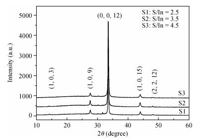
Fig. 1.
X-ray diffraction patterns of S1, S2 and S3 films
SEMICONDUCTOR MATERIALS
Thierno Sall1, 2, A. Nafidi4, Bernabé Marí Soucase2, , Miguel Mollar2, Bouchaib Hartitti3 and Mounir Fahoume1
Corresponding author: Bernabé Marí Soucase, Email:bmari@fis.upv.es
Abstract: Indium sulfide (In2S3) thin films were prepared by chemical spray pyrolysis technique from solutions with different[S]/[In] ratios on glass substrates at a constant temperature of 250℃. Thin films were characterized by X-ray diffraction (XRD), scanning electron microscopy (SEM), atomic force microscopy (AFM), energy dispersive X-ray spectroscopy (EDS), Raman spectroscopy and optical transmittance spectroscopy. All samples exhibit a polycrystalline structure with a preferential orientation along (0, 0, 12). A good stoichiometry was attained for all samples. The morphology of thin film surfaces, as seen by SEM, was dense and no cracks or pinholes were observed. Raman spectroscopy analysis shows active modes belonging to β-ln2S3 phase. The optical transmittance in the visible range is higher than 60% and the band gap energy slightly increases with the sulfur to indium ratio, attaining a value of 2.63 eV for[S]/[In]=4.5.
Keywords: In2S3, thin films, spray pyrolysis, [S]/[In] ratio, AFM, Raman spectroscopy
| [1] |
Shay J L, Tell B. Energy band structure of Ⅰ-Ⅲ-Ⅵ2 semiconductors. Surf Sci, 1973, 37:748 doi: 10.1016/0039-6028(73)90364-6
|
| [2] |
George J, Joseph K S, Prodeep B, et al. Reactivity evaporated film of indium sulfide. Phys Status Solidi, Appl Res, 1988, 106:123 doi: 10.1002/(ISSN)1521-396X
|
| [3] |
Barreau N, Bernede J C, Marsillac S, et al. New Cd-free buffer layer deposited by PVD:In2S3 containing Na compounds. Thin Solid Films, 2003, 431:326
|
| [4] |
Bube R H, McCarroll W H. Photoconductivity in indium sulfide powders and crystal. J Phys Chem Solids, 1959, 10:333 doi: 10.1016/0022-3697(59)90010-1
|
| [5] |
Buecheler S, Corica D, Guettler D, et al. Ultrasonically sprayed indium sulfide buffer layers for Cu(In, Ga)(S, Se)2 thin-film solar cells. Thin Solid Films, 2009, 517(7):2312 doi: 10.1016/j.tsf.2008.10.135
|
| [6] |
Sall T, Raidou A, Elfarrass S, et al. Structural, morphological and optical properties of In2S3 thin films obtained by SILAR method. Opt Quant Electron, 2014, 46(1):247 doi: 10.1007/s11082-013-9786-x
|
| [7] |
Shazly A A E L, Abdelkady D, Metoually H S, et al. Electrical properties of β -In2S3 thin films. J Phys Condens Matter, 1998, 10:5943 doi: 10.1088/0953-8984/10/26/019
|
| [8] |
Asikainen T, Ritala M, Leskela M. Growth of In2S3 thin films by atomic layer epitaxy. Appl Surf Sci, 1994, 82:122
|
| [9] |
Dedova T, Wienke J, Goris M, et al. Characterization of the chemical deposited In(OH)xSy films:effect of the growth conditions. Thin Solid Films, 2007, 515:6064 doi: 10.1016/j.tsf.2006.12.146
|
| [10] |
Sall T, Hartiti B, Marí B, et al. Elaboration and characterization of In2S3 thin films by spray pyrolysis with[S]/[In]=3 ratio. IEEE International Renewable and Sustainable Energy Conference (IRSEC), 2013:58
|
| [11] |
Yasaki Y, Sonoyama N, Sakata T. Semiconductor sensitization of coloidal In2S3 on wide gap semiconductors. J Electroanal Chem, 1999, 469:116 doi: 10.1016/S0022-0728(99)00184-9
|
| [12] |
Marí B, Mollar M, Soro D, et al. Electrodeposition of In2S3 thin films onto FTO substrate from DMSO solution. Int J Electrochem Sci, 2013, 8:3510
|
| [13] |
Bayon R, Guillén C, Martinez M A, et al. Preparation of indium hydroxy sulfide Inx(OH)ySz thin films by chemical bath deposition. Electrochem Soc, 1998, 145:2775 doi: 10.1149/1.1838713
|
| [14] |
Perednis D, Gauckler L J. Thin film deposition using spray pyrolysis. Journal of Electroceramics, 2005, 14:103 doi: 10.1007/s10832-005-0870-x
|
| [15] |
Otto K, Katerski A, Volobujeva O, et al. Indium sulfide thin films deposited by chemical spray aqueous and alcoholic solutions. Energy Procedia, 2011, 3:63 doi: 10.1016/j.egypro.2011.01.011
|
| [16] |
Spasevska H, Kitts C C, Ancora C, et al. Optimised In2S3 thin films deposited by spray pyrolysis. International Journal of Photoenergy, 2012, 2012:1
|
| [17] |
John T T, Kartha C S, Vijayakumar K P, et al. Preparation of indium sulfide thin films by spray pyrolysis using a new precursor indium nitrate. Appl Surf Sci, 2005, 252:1360 doi: 10.1016/j.apsusc.2005.02.093
|
| [18] |
Barreau N, MarsilIac S, Albertini D, et al. Structural, optical and electrical properties of β-In2S3-3xO3x thin films obtained by PVD. Thin Solid Films, 2002, 403/404:331
|
| [19] |
Kim W T, Kim C D. Optical energy gaps of β-In2S3 thin films grown by spray pyrolysis. J Appl Phys, 1986, 60(7):2631 doi: 10.1063/1.337137
|
| [20] |
Yasaki Y, Csonoyama N, Sakata T. Semiconductor sensitization of colloidal In2S3 on wide gap semiconductors. J Electroanal Chem, 1999, 469(2):116 doi: 10.1016/S0022-0728(99)00184-9
|
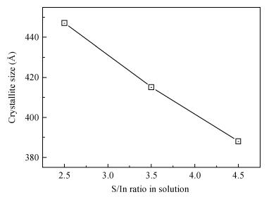
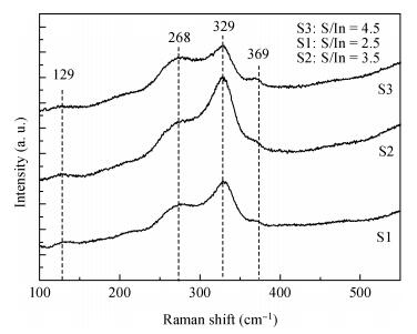
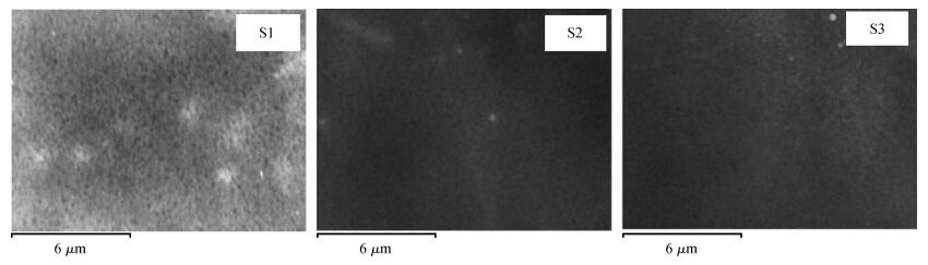
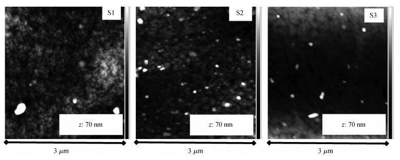
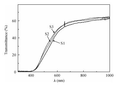
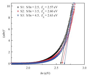
Table 1. Grain size and surface roughness of samples using AFM analysis

|
Table 2. [S]/[In] ratios in solution and S/In in the solid thin film as measured by EDS

|
Table 3. Band gap energy of sprayed In2S3 thin films

|
| [1] |
Shay J L, Tell B. Energy band structure of Ⅰ-Ⅲ-Ⅵ2 semiconductors. Surf Sci, 1973, 37:748 doi: 10.1016/0039-6028(73)90364-6
|
| [2] |
George J, Joseph K S, Prodeep B, et al. Reactivity evaporated film of indium sulfide. Phys Status Solidi, Appl Res, 1988, 106:123 doi: 10.1002/(ISSN)1521-396X
|
| [3] |
Barreau N, Bernede J C, Marsillac S, et al. New Cd-free buffer layer deposited by PVD:In2S3 containing Na compounds. Thin Solid Films, 2003, 431:326
|
| [4] |
Bube R H, McCarroll W H. Photoconductivity in indium sulfide powders and crystal. J Phys Chem Solids, 1959, 10:333 doi: 10.1016/0022-3697(59)90010-1
|
| [5] |
Buecheler S, Corica D, Guettler D, et al. Ultrasonically sprayed indium sulfide buffer layers for Cu(In, Ga)(S, Se)2 thin-film solar cells. Thin Solid Films, 2009, 517(7):2312 doi: 10.1016/j.tsf.2008.10.135
|
| [6] |
Sall T, Raidou A, Elfarrass S, et al. Structural, morphological and optical properties of In2S3 thin films obtained by SILAR method. Opt Quant Electron, 2014, 46(1):247 doi: 10.1007/s11082-013-9786-x
|
| [7] |
Shazly A A E L, Abdelkady D, Metoually H S, et al. Electrical properties of β -In2S3 thin films. J Phys Condens Matter, 1998, 10:5943 doi: 10.1088/0953-8984/10/26/019
|
| [8] |
Asikainen T, Ritala M, Leskela M. Growth of In2S3 thin films by atomic layer epitaxy. Appl Surf Sci, 1994, 82:122
|
| [9] |
Dedova T, Wienke J, Goris M, et al. Characterization of the chemical deposited In(OH)xSy films:effect of the growth conditions. Thin Solid Films, 2007, 515:6064 doi: 10.1016/j.tsf.2006.12.146
|
| [10] |
Sall T, Hartiti B, Marí B, et al. Elaboration and characterization of In2S3 thin films by spray pyrolysis with[S]/[In]=3 ratio. IEEE International Renewable and Sustainable Energy Conference (IRSEC), 2013:58
|
| [11] |
Yasaki Y, Sonoyama N, Sakata T. Semiconductor sensitization of coloidal In2S3 on wide gap semiconductors. J Electroanal Chem, 1999, 469:116 doi: 10.1016/S0022-0728(99)00184-9
|
| [12] |
Marí B, Mollar M, Soro D, et al. Electrodeposition of In2S3 thin films onto FTO substrate from DMSO solution. Int J Electrochem Sci, 2013, 8:3510
|
| [13] |
Bayon R, Guillén C, Martinez M A, et al. Preparation of indium hydroxy sulfide Inx(OH)ySz thin films by chemical bath deposition. Electrochem Soc, 1998, 145:2775 doi: 10.1149/1.1838713
|
| [14] |
Perednis D, Gauckler L J. Thin film deposition using spray pyrolysis. Journal of Electroceramics, 2005, 14:103 doi: 10.1007/s10832-005-0870-x
|
| [15] |
Otto K, Katerski A, Volobujeva O, et al. Indium sulfide thin films deposited by chemical spray aqueous and alcoholic solutions. Energy Procedia, 2011, 3:63 doi: 10.1016/j.egypro.2011.01.011
|
| [16] |
Spasevska H, Kitts C C, Ancora C, et al. Optimised In2S3 thin films deposited by spray pyrolysis. International Journal of Photoenergy, 2012, 2012:1
|
| [17] |
John T T, Kartha C S, Vijayakumar K P, et al. Preparation of indium sulfide thin films by spray pyrolysis using a new precursor indium nitrate. Appl Surf Sci, 2005, 252:1360 doi: 10.1016/j.apsusc.2005.02.093
|
| [18] |
Barreau N, MarsilIac S, Albertini D, et al. Structural, optical and electrical properties of β-In2S3-3xO3x thin films obtained by PVD. Thin Solid Films, 2002, 403/404:331
|
| [19] |
Kim W T, Kim C D. Optical energy gaps of β-In2S3 thin films grown by spray pyrolysis. J Appl Phys, 1986, 60(7):2631 doi: 10.1063/1.337137
|
| [20] |
Yasaki Y, Csonoyama N, Sakata T. Semiconductor sensitization of colloidal In2S3 on wide gap semiconductors. J Electroanal Chem, 1999, 469(2):116 doi: 10.1016/S0022-0728(99)00184-9
|


Article views: 3635 Times PDF downloads: 42 Times Cited by: 0 Times
Received: 03 September 2013 Revised: 23 January 2014 Online: Published: 01 June 2014
| Citation: |
Thierno Sall, A. Nafidi, Bernabé Marí Soucase, Miguel Mollar, Bouchaib Hartitti, Mounir Fahoume. Synthesis of In2S3 thin films by spray pyrolysis from precursors with different[S]/[In] ratios[J]. Journal of Semiconductors, 2014, 35(6): 063002. doi: 10.1088/1674-4926/35/6/063002
****
T Sall, A. Nafidi, B M Soucase, M Mollar, B Hartitti, M Fahoume. Synthesis of In2S3 thin films by spray pyrolysis from precursors with different[S]/[In] ratios[J]. J. Semicond., 2014, 35(6): 063002. doi: 10.1088/1674-4926/35/6/063002.

|
| [1] |
Shay J L, Tell B. Energy band structure of Ⅰ-Ⅲ-Ⅵ2 semiconductors. Surf Sci, 1973, 37:748 doi: 10.1016/0039-6028(73)90364-6
|
| [2] |
George J, Joseph K S, Prodeep B, et al. Reactivity evaporated film of indium sulfide. Phys Status Solidi, Appl Res, 1988, 106:123 doi: 10.1002/(ISSN)1521-396X
|
| [3] |
Barreau N, Bernede J C, Marsillac S, et al. New Cd-free buffer layer deposited by PVD:In2S3 containing Na compounds. Thin Solid Films, 2003, 431:326
|
| [4] |
Bube R H, McCarroll W H. Photoconductivity in indium sulfide powders and crystal. J Phys Chem Solids, 1959, 10:333 doi: 10.1016/0022-3697(59)90010-1
|
| [5] |
Buecheler S, Corica D, Guettler D, et al. Ultrasonically sprayed indium sulfide buffer layers for Cu(In, Ga)(S, Se)2 thin-film solar cells. Thin Solid Films, 2009, 517(7):2312 doi: 10.1016/j.tsf.2008.10.135
|
| [6] |
Sall T, Raidou A, Elfarrass S, et al. Structural, morphological and optical properties of In2S3 thin films obtained by SILAR method. Opt Quant Electron, 2014, 46(1):247 doi: 10.1007/s11082-013-9786-x
|
| [7] |
Shazly A A E L, Abdelkady D, Metoually H S, et al. Electrical properties of β -In2S3 thin films. J Phys Condens Matter, 1998, 10:5943 doi: 10.1088/0953-8984/10/26/019
|
| [8] |
Asikainen T, Ritala M, Leskela M. Growth of In2S3 thin films by atomic layer epitaxy. Appl Surf Sci, 1994, 82:122
|
| [9] |
Dedova T, Wienke J, Goris M, et al. Characterization of the chemical deposited In(OH)xSy films:effect of the growth conditions. Thin Solid Films, 2007, 515:6064 doi: 10.1016/j.tsf.2006.12.146
|
| [10] |
Sall T, Hartiti B, Marí B, et al. Elaboration and characterization of In2S3 thin films by spray pyrolysis with[S]/[In]=3 ratio. IEEE International Renewable and Sustainable Energy Conference (IRSEC), 2013:58
|
| [11] |
Yasaki Y, Sonoyama N, Sakata T. Semiconductor sensitization of coloidal In2S3 on wide gap semiconductors. J Electroanal Chem, 1999, 469:116 doi: 10.1016/S0022-0728(99)00184-9
|
| [12] |
Marí B, Mollar M, Soro D, et al. Electrodeposition of In2S3 thin films onto FTO substrate from DMSO solution. Int J Electrochem Sci, 2013, 8:3510
|
| [13] |
Bayon R, Guillén C, Martinez M A, et al. Preparation of indium hydroxy sulfide Inx(OH)ySz thin films by chemical bath deposition. Electrochem Soc, 1998, 145:2775 doi: 10.1149/1.1838713
|
| [14] |
Perednis D, Gauckler L J. Thin film deposition using spray pyrolysis. Journal of Electroceramics, 2005, 14:103 doi: 10.1007/s10832-005-0870-x
|
| [15] |
Otto K, Katerski A, Volobujeva O, et al. Indium sulfide thin films deposited by chemical spray aqueous and alcoholic solutions. Energy Procedia, 2011, 3:63 doi: 10.1016/j.egypro.2011.01.011
|
| [16] |
Spasevska H, Kitts C C, Ancora C, et al. Optimised In2S3 thin films deposited by spray pyrolysis. International Journal of Photoenergy, 2012, 2012:1
|
| [17] |
John T T, Kartha C S, Vijayakumar K P, et al. Preparation of indium sulfide thin films by spray pyrolysis using a new precursor indium nitrate. Appl Surf Sci, 2005, 252:1360 doi: 10.1016/j.apsusc.2005.02.093
|
| [18] |
Barreau N, MarsilIac S, Albertini D, et al. Structural, optical and electrical properties of β-In2S3-3xO3x thin films obtained by PVD. Thin Solid Films, 2002, 403/404:331
|
| [19] |
Kim W T, Kim C D. Optical energy gaps of β-In2S3 thin films grown by spray pyrolysis. J Appl Phys, 1986, 60(7):2631 doi: 10.1063/1.337137
|
| [20] |
Yasaki Y, Csonoyama N, Sakata T. Semiconductor sensitization of colloidal In2S3 on wide gap semiconductors. J Electroanal Chem, 1999, 469(2):116 doi: 10.1016/S0022-0728(99)00184-9
|

 WeChat ID
Journal of Semiconductors © 2017 All Rights Reserved 京ICP备05085259号-2

 DownLoad:

