


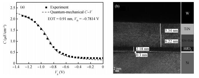
Fig. 1.
(a) High frequency C-V ($f=$ 100 kHz) curve of 16 × 8 $\mu $ m2 transistors in the depletion and accumulation region. (b) The TEM image of the gate stack with 0.3 nm interfacial SiO2 and 2.18 nm HfO2
SEMICONDUCTOR DEVICES
Fenfen Tao1, 2, Hong Yang2, Bo Tang2, Zhaoyun Tang2, Yefeng Xu2, Jing Xu2, Qingpu Wang1, and Jiang Yan2
Corresponding author: Wang Qingpu, Email:wangqingpu@sdu.edu.cn
Abstract: The characteristics of TDDB (time-dependent dielectric breakdown) and SILC (stress-induced leakage current) for an ultra-thin SiO2/HfO2 gate dielectric stack are studied. The EOT (equivalent-oxide-thickness) of the gate stack (Si/SiO2/HfO2/TiN/TiAl/TiN/W) is 0.91 nm. The field acceleration factor (γ) extracted in TDDB experiments is 1.59 s·cm/MV, and the maximum voltage is 1.06 V when the devices operate at 125℃ for ten years. A detailed study on the defect generation mechanism induced by SILC is presented to deeply understand the breakdown behavior. The trap energy levels can be calculated by the SILC peaks:one SILC peak is most likely to be caused by the neutral oxygen vacancy (VO) in the HfO2 bulk layer at 0.51 eV below the Si conduction band minimum; another SILC peak is induced by the interface traps, which are aligned with the silicon conduction band edge. Furthermore, the great difference between the two SILC peaks demonstrates that the degeneration of the high-k layer dominates the breakdown behavior of the extremely thin gate dielectric.
Keywords: HfO2, TDDB, SILC, bulk trap, interface trap
| [1] |
Xin Weiping, Zhuang Yiqi, Li Xiaoming, et al. An embeddable SOC real-time prediction technology for TDDB. Journal of Semiconductors, 2012, 33(11):115009 doi: 10.1088/1674-4926/33/11/115009
|
| [2] |
Hu Shigang, Hao Yue, Ma Xiaohua, et al. Degradation of nMOS and pMOSFETs with ultrathin gate oxide under DT stress. Journal of Semiconductors, 2008, 29(11):2136 http://www.jos.ac.cn/bdtxben/ch/reader/view_abstract.aspx?file_no=08051603&flag=1
|
| [3] |
O'Connor R, Pantisano L, Degraeve R, et al. SILC defect generation spectroscopy in HfSiON using constant voltage stress and substrate hot electron injection. International Reliability Physics Symposium (IRPS), 2008:324 https://lirias.kuleuven.be/handle/123456789/303389
|
| [4] |
Cao Yanrong, Ma Xiaohua, Hao Yue, et al. Models and related mechanisms of NBTI degradation of 90 nm pMOSFETs. Chinese Journal of Semiconductors, 2007, 28(5):665 http://www.jos.ac.cn/bdtxben/ch/reader/view_abstract.aspx?file_no=06111602&flag=1
|
| [5] |
Cartier E, Kerber A. Stress-induced leakage current and defect generation in nFETs with HfO2/TiN gate stacks during positive-bias temperature stress. International Reliability Physics Symposium (IRPS), 2009:486
|
| [6] |
Yang J, Masuduzzaman M, Joshi K, et al. Intrinsic correlation between PBTI and TDDB degradations in nMOS HK/MG dielectrics. International Reliability Physics Symposium (IRPS), 2012:5D.4.1 http://ieeexplore.ieee.org/document/6241855/
|
| [7] |
Pae S, Ashok A, Choi J, et al. Reliability characterization of 32 nm high-k and metal-gate logic transistor technology. International Reliability Physics Symposium (IRPS), 2010:287
|
| [8] |
Petit C, Meinertzhagen A, Zander D, et al. Low voltage SILC and P-and N-MOSFET gateoxide reliability. Microelectron Reliab, 2005, 45(3/4):479
|
| [9] |
Kim Y H, Lee J C. Reliability characteristics of high-k dielectrics. Microelectron Reliab, 2004, 44(2):183 doi: 10.1016/j.microrel.2003.10.008
|
| [10] |
Degraeve R, Groeseneken G, Bellens R, et al. New insights in the relation between electron trap generation and the statistical properties of oxide breakdown. IEEE Trans Electron Devices, 1998, 45(4):904 doi: 10.1109/16.662800
|
| [11] |
Degraeve R, Kauerauf T, Cho M, et al. Degradation and breakdown of 0.9 nm EOT SiO2/ALD HfO2/metal gate stacks under positive constant voltage stress. IEEE International Electron Devices Meeting (IEDM), 2005:419
|
| [12] |
Bera M K, Mahata C, Mait C K. Reliability of ultra-thin titanium dioxide (TiO2) films on strained-Si. Thin Solid Films, 2008, 517(1):27 doi: 10.1016/j.tsf.2008.08.008
|
| [13] |
McPherson J W. Time dependent dielectric breakdown physics-models revisited. Microelectron Reliab, 2012, 52(9/10):1753
|
| [14] |
McPherson J W, Mogul H C. Underlying physics of the thermochemical E model in describing low-field time-dependent dielectric breakdown in SiO2 thin films. Appl Phys Lett, 1998, 84(3):1513
|
| [15] |
McPherson J, Kim J Y, Shanware A, et al. Thermochemical description of dielectric breakdown in high dielectricconstant materials. Appl Phys Lett, 2003, 82(13):2121 doi: 10.1063/1.1565180
|
| [16] |
Arora N. MOSFET models for VLSI circuit simulation:theory and practice. New York:Springer-Verlag, 1993:236
|
| [17] |
Prégaldiny F, Lallement C, van Langevelde R, et al. An advanced explicit surface potential model physically accounting for the quantization effects in deep-submicron MOSFETs. Solid-State Electron, 2004, 48(3):427 doi: 10.1016/j.sse.2003.09.005
|
| [18] |
Wilk G D, Wallace R M, Anthony J M. High-k gate dielectrics:current status and materials properties considerations. J Appl Phys, 2001, 89(10):5243 doi: 10.1063/1.1361065
|
| [19] |
Xiong K, Robertson J, Gibson M C, et al. Defect energy levels in HfO2 high-dielectric-constant gate oxide. Appl Phys Lett, 2005, 87(18):183505 doi: 10.1063/1.2119425
|
| [20] |
O'Sullivan B J, Hurley P K, Leveugle C, et al. Si (100)-SiO2 interface properties following rapid thermal processing. J Appl Phys, 2001, 89(7):3811 doi: 10.1063/1.1343897
|
| [21] |
Sahhaf S, Degraeve R, O'Connor R, et al. Evidence of a new degradation mechanism in high-k dielectrics at elevated temperatures. International Reliability Physics Symposium (IRPS), 2009:493 http://ieeexplore.ieee.org/document/5173302/authors
|
| [22] |
Bersuker G, Heh D, Young C, et al. Breakdown in the metal/high-k gate stack:identifying the weak link in the multilayer dielectric. IEEE International Electron Devices Meeting (IEDM), 2008:791
|
| [23] |
Chowdhury N A, Bersuker G, Young C, et al. Breakdown characteristics of nFETs in inversion with metal/HfO2 gate stacks. Microelectron Eng, 2008, 85(1):27 doi: 10.1016/j.mee.2007.01.173
|
| [24] |
Degraeve R, Kerber A, Roussel P, et al. Effect of bulk trap density on HfO2 reliability and yield. IEEE International Electron Devices Meeting (IEDM), 2003:38.5.1
|
| [25] |
Okada K, Ota H, Hirano A, et al. Roles of high-k and interfacial layers on TDDB reliability studied with HfAlOx/SiO2 stacked gate dielectrics. International Reliability Physics Symposium (IRPS), 2008:661
|
| [26] |
Kimmel A V, Sushko P V, Shluger A L, et al. Positive and negative oxygen vacancies in amorphous silica. Electrochemical Society Transactions, 2009, 19(2):3
|
| [27] |
Vandelli L, Padovani A, Larcher L, et al. A physical model of the temperature dependence of the current through SiO2/HfO2 stacks. IEEE Trans Electron Devices, 2011, 58(9):2878 doi: 10.1109/TED.2011.2158825
|
| [28] |
Muñoz Ramo D, Gavartin J L, Shluger A L, et al. Spectroscopic properties of oxygen vacancies in monoclinic HfO2 calculated with periodic and embedded cluster density functional theory. Phys Rev B, 2007, 75(20):205
|
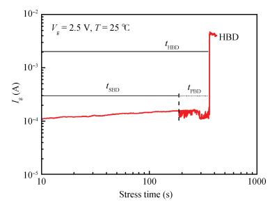
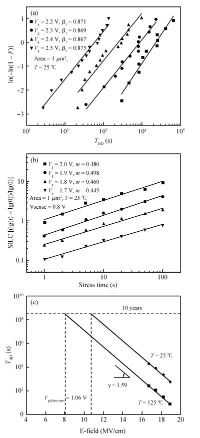
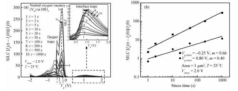
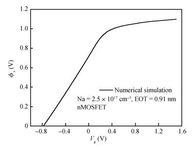
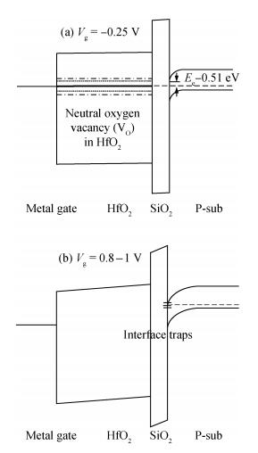
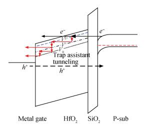
Table 1. The basic parameters of materials

|
| [1] |
Xin Weiping, Zhuang Yiqi, Li Xiaoming, et al. An embeddable SOC real-time prediction technology for TDDB. Journal of Semiconductors, 2012, 33(11):115009 doi: 10.1088/1674-4926/33/11/115009
|
| [2] |
Hu Shigang, Hao Yue, Ma Xiaohua, et al. Degradation of nMOS and pMOSFETs with ultrathin gate oxide under DT stress. Journal of Semiconductors, 2008, 29(11):2136 http://www.jos.ac.cn/bdtxben/ch/reader/view_abstract.aspx?file_no=08051603&flag=1
|
| [3] |
O'Connor R, Pantisano L, Degraeve R, et al. SILC defect generation spectroscopy in HfSiON using constant voltage stress and substrate hot electron injection. International Reliability Physics Symposium (IRPS), 2008:324 https://lirias.kuleuven.be/handle/123456789/303389
|
| [4] |
Cao Yanrong, Ma Xiaohua, Hao Yue, et al. Models and related mechanisms of NBTI degradation of 90 nm pMOSFETs. Chinese Journal of Semiconductors, 2007, 28(5):665 http://www.jos.ac.cn/bdtxben/ch/reader/view_abstract.aspx?file_no=06111602&flag=1
|
| [5] |
Cartier E, Kerber A. Stress-induced leakage current and defect generation in nFETs with HfO2/TiN gate stacks during positive-bias temperature stress. International Reliability Physics Symposium (IRPS), 2009:486
|
| [6] |
Yang J, Masuduzzaman M, Joshi K, et al. Intrinsic correlation between PBTI and TDDB degradations in nMOS HK/MG dielectrics. International Reliability Physics Symposium (IRPS), 2012:5D.4.1 http://ieeexplore.ieee.org/document/6241855/
|
| [7] |
Pae S, Ashok A, Choi J, et al. Reliability characterization of 32 nm high-k and metal-gate logic transistor technology. International Reliability Physics Symposium (IRPS), 2010:287
|
| [8] |
Petit C, Meinertzhagen A, Zander D, et al. Low voltage SILC and P-and N-MOSFET gateoxide reliability. Microelectron Reliab, 2005, 45(3/4):479
|
| [9] |
Kim Y H, Lee J C. Reliability characteristics of high-k dielectrics. Microelectron Reliab, 2004, 44(2):183 doi: 10.1016/j.microrel.2003.10.008
|
| [10] |
Degraeve R, Groeseneken G, Bellens R, et al. New insights in the relation between electron trap generation and the statistical properties of oxide breakdown. IEEE Trans Electron Devices, 1998, 45(4):904 doi: 10.1109/16.662800
|
| [11] |
Degraeve R, Kauerauf T, Cho M, et al. Degradation and breakdown of 0.9 nm EOT SiO2/ALD HfO2/metal gate stacks under positive constant voltage stress. IEEE International Electron Devices Meeting (IEDM), 2005:419
|
| [12] |
Bera M K, Mahata C, Mait C K. Reliability of ultra-thin titanium dioxide (TiO2) films on strained-Si. Thin Solid Films, 2008, 517(1):27 doi: 10.1016/j.tsf.2008.08.008
|
| [13] |
McPherson J W. Time dependent dielectric breakdown physics-models revisited. Microelectron Reliab, 2012, 52(9/10):1753
|
| [14] |
McPherson J W, Mogul H C. Underlying physics of the thermochemical E model in describing low-field time-dependent dielectric breakdown in SiO2 thin films. Appl Phys Lett, 1998, 84(3):1513
|
| [15] |
McPherson J, Kim J Y, Shanware A, et al. Thermochemical description of dielectric breakdown in high dielectricconstant materials. Appl Phys Lett, 2003, 82(13):2121 doi: 10.1063/1.1565180
|
| [16] |
Arora N. MOSFET models for VLSI circuit simulation:theory and practice. New York:Springer-Verlag, 1993:236
|
| [17] |
Prégaldiny F, Lallement C, van Langevelde R, et al. An advanced explicit surface potential model physically accounting for the quantization effects in deep-submicron MOSFETs. Solid-State Electron, 2004, 48(3):427 doi: 10.1016/j.sse.2003.09.005
|
| [18] |
Wilk G D, Wallace R M, Anthony J M. High-k gate dielectrics:current status and materials properties considerations. J Appl Phys, 2001, 89(10):5243 doi: 10.1063/1.1361065
|
| [19] |
Xiong K, Robertson J, Gibson M C, et al. Defect energy levels in HfO2 high-dielectric-constant gate oxide. Appl Phys Lett, 2005, 87(18):183505 doi: 10.1063/1.2119425
|
| [20] |
O'Sullivan B J, Hurley P K, Leveugle C, et al. Si (100)-SiO2 interface properties following rapid thermal processing. J Appl Phys, 2001, 89(7):3811 doi: 10.1063/1.1343897
|
| [21] |
Sahhaf S, Degraeve R, O'Connor R, et al. Evidence of a new degradation mechanism in high-k dielectrics at elevated temperatures. International Reliability Physics Symposium (IRPS), 2009:493 http://ieeexplore.ieee.org/document/5173302/authors
|
| [22] |
Bersuker G, Heh D, Young C, et al. Breakdown in the metal/high-k gate stack:identifying the weak link in the multilayer dielectric. IEEE International Electron Devices Meeting (IEDM), 2008:791
|
| [23] |
Chowdhury N A, Bersuker G, Young C, et al. Breakdown characteristics of nFETs in inversion with metal/HfO2 gate stacks. Microelectron Eng, 2008, 85(1):27 doi: 10.1016/j.mee.2007.01.173
|
| [24] |
Degraeve R, Kerber A, Roussel P, et al. Effect of bulk trap density on HfO2 reliability and yield. IEEE International Electron Devices Meeting (IEDM), 2003:38.5.1
|
| [25] |
Okada K, Ota H, Hirano A, et al. Roles of high-k and interfacial layers on TDDB reliability studied with HfAlOx/SiO2 stacked gate dielectrics. International Reliability Physics Symposium (IRPS), 2008:661
|
| [26] |
Kimmel A V, Sushko P V, Shluger A L, et al. Positive and negative oxygen vacancies in amorphous silica. Electrochemical Society Transactions, 2009, 19(2):3
|
| [27] |
Vandelli L, Padovani A, Larcher L, et al. A physical model of the temperature dependence of the current through SiO2/HfO2 stacks. IEEE Trans Electron Devices, 2011, 58(9):2878 doi: 10.1109/TED.2011.2158825
|
| [28] |
Muñoz Ramo D, Gavartin J L, Shluger A L, et al. Spectroscopic properties of oxygen vacancies in monoclinic HfO2 calculated with periodic and embedded cluster density functional theory. Phys Rev B, 2007, 75(20):205
|


Article views: 7693 Times PDF downloads: 609 Times Cited by: 0 Times
Received: 12 December 2013 Revised: 27 January 2014 Online: Published: 01 June 2014
| Citation: |
Fenfen Tao, Hong Yang, Bo Tang, Zhaoyun Tang, Yefeng Xu, Jing Xu, Qingpu Wang, Jiang Yan. TDDB characteristic and breakdown mechanism of ultra-thin SiO2/HfO2 bilayer gate dielectrics[J]. Journal of Semiconductors, 2014, 35(6): 064003. doi: 10.1088/1674-4926/35/6/064003
****
F F Tao, H Yang, B Tang, Z Y Tang, Y F Xu, J Xu, Q P Wang, J Yan. TDDB characteristic and breakdown mechanism of ultra-thin SiO2/HfO2 bilayer gate dielectrics[J]. J. Semicond., 2014, 35(6): 064003. doi: 10.1088/1674-4926/35/6/064003.

|
| [1] |
Xin Weiping, Zhuang Yiqi, Li Xiaoming, et al. An embeddable SOC real-time prediction technology for TDDB. Journal of Semiconductors, 2012, 33(11):115009 doi: 10.1088/1674-4926/33/11/115009
|
| [2] |
Hu Shigang, Hao Yue, Ma Xiaohua, et al. Degradation of nMOS and pMOSFETs with ultrathin gate oxide under DT stress. Journal of Semiconductors, 2008, 29(11):2136 http://www.jos.ac.cn/bdtxben/ch/reader/view_abstract.aspx?file_no=08051603&flag=1
|
| [3] |
O'Connor R, Pantisano L, Degraeve R, et al. SILC defect generation spectroscopy in HfSiON using constant voltage stress and substrate hot electron injection. International Reliability Physics Symposium (IRPS), 2008:324 https://lirias.kuleuven.be/handle/123456789/303389
|
| [4] |
Cao Yanrong, Ma Xiaohua, Hao Yue, et al. Models and related mechanisms of NBTI degradation of 90 nm pMOSFETs. Chinese Journal of Semiconductors, 2007, 28(5):665 http://www.jos.ac.cn/bdtxben/ch/reader/view_abstract.aspx?file_no=06111602&flag=1
|
| [5] |
Cartier E, Kerber A. Stress-induced leakage current and defect generation in nFETs with HfO2/TiN gate stacks during positive-bias temperature stress. International Reliability Physics Symposium (IRPS), 2009:486
|
| [6] |
Yang J, Masuduzzaman M, Joshi K, et al. Intrinsic correlation between PBTI and TDDB degradations in nMOS HK/MG dielectrics. International Reliability Physics Symposium (IRPS), 2012:5D.4.1 http://ieeexplore.ieee.org/document/6241855/
|
| [7] |
Pae S, Ashok A, Choi J, et al. Reliability characterization of 32 nm high-k and metal-gate logic transistor technology. International Reliability Physics Symposium (IRPS), 2010:287
|
| [8] |
Petit C, Meinertzhagen A, Zander D, et al. Low voltage SILC and P-and N-MOSFET gateoxide reliability. Microelectron Reliab, 2005, 45(3/4):479
|
| [9] |
Kim Y H, Lee J C. Reliability characteristics of high-k dielectrics. Microelectron Reliab, 2004, 44(2):183 doi: 10.1016/j.microrel.2003.10.008
|
| [10] |
Degraeve R, Groeseneken G, Bellens R, et al. New insights in the relation between electron trap generation and the statistical properties of oxide breakdown. IEEE Trans Electron Devices, 1998, 45(4):904 doi: 10.1109/16.662800
|
| [11] |
Degraeve R, Kauerauf T, Cho M, et al. Degradation and breakdown of 0.9 nm EOT SiO2/ALD HfO2/metal gate stacks under positive constant voltage stress. IEEE International Electron Devices Meeting (IEDM), 2005:419
|
| [12] |
Bera M K, Mahata C, Mait C K. Reliability of ultra-thin titanium dioxide (TiO2) films on strained-Si. Thin Solid Films, 2008, 517(1):27 doi: 10.1016/j.tsf.2008.08.008
|
| [13] |
McPherson J W. Time dependent dielectric breakdown physics-models revisited. Microelectron Reliab, 2012, 52(9/10):1753
|
| [14] |
McPherson J W, Mogul H C. Underlying physics of the thermochemical E model in describing low-field time-dependent dielectric breakdown in SiO2 thin films. Appl Phys Lett, 1998, 84(3):1513
|
| [15] |
McPherson J, Kim J Y, Shanware A, et al. Thermochemical description of dielectric breakdown in high dielectricconstant materials. Appl Phys Lett, 2003, 82(13):2121 doi: 10.1063/1.1565180
|
| [16] |
Arora N. MOSFET models for VLSI circuit simulation:theory and practice. New York:Springer-Verlag, 1993:236
|
| [17] |
Prégaldiny F, Lallement C, van Langevelde R, et al. An advanced explicit surface potential model physically accounting for the quantization effects in deep-submicron MOSFETs. Solid-State Electron, 2004, 48(3):427 doi: 10.1016/j.sse.2003.09.005
|
| [18] |
Wilk G D, Wallace R M, Anthony J M. High-k gate dielectrics:current status and materials properties considerations. J Appl Phys, 2001, 89(10):5243 doi: 10.1063/1.1361065
|
| [19] |
Xiong K, Robertson J, Gibson M C, et al. Defect energy levels in HfO2 high-dielectric-constant gate oxide. Appl Phys Lett, 2005, 87(18):183505 doi: 10.1063/1.2119425
|
| [20] |
O'Sullivan B J, Hurley P K, Leveugle C, et al. Si (100)-SiO2 interface properties following rapid thermal processing. J Appl Phys, 2001, 89(7):3811 doi: 10.1063/1.1343897
|
| [21] |
Sahhaf S, Degraeve R, O'Connor R, et al. Evidence of a new degradation mechanism in high-k dielectrics at elevated temperatures. International Reliability Physics Symposium (IRPS), 2009:493 http://ieeexplore.ieee.org/document/5173302/authors
|
| [22] |
Bersuker G, Heh D, Young C, et al. Breakdown in the metal/high-k gate stack:identifying the weak link in the multilayer dielectric. IEEE International Electron Devices Meeting (IEDM), 2008:791
|
| [23] |
Chowdhury N A, Bersuker G, Young C, et al. Breakdown characteristics of nFETs in inversion with metal/HfO2 gate stacks. Microelectron Eng, 2008, 85(1):27 doi: 10.1016/j.mee.2007.01.173
|
| [24] |
Degraeve R, Kerber A, Roussel P, et al. Effect of bulk trap density on HfO2 reliability and yield. IEEE International Electron Devices Meeting (IEDM), 2003:38.5.1
|
| [25] |
Okada K, Ota H, Hirano A, et al. Roles of high-k and interfacial layers on TDDB reliability studied with HfAlOx/SiO2 stacked gate dielectrics. International Reliability Physics Symposium (IRPS), 2008:661
|
| [26] |
Kimmel A V, Sushko P V, Shluger A L, et al. Positive and negative oxygen vacancies in amorphous silica. Electrochemical Society Transactions, 2009, 19(2):3
|
| [27] |
Vandelli L, Padovani A, Larcher L, et al. A physical model of the temperature dependence of the current through SiO2/HfO2 stacks. IEEE Trans Electron Devices, 2011, 58(9):2878 doi: 10.1109/TED.2011.2158825
|
| [28] |
Muñoz Ramo D, Gavartin J L, Shluger A L, et al. Spectroscopic properties of oxygen vacancies in monoclinic HfO2 calculated with periodic and embedded cluster density functional theory. Phys Rev B, 2007, 75(20):205
|

 WeChat ID
Journal of Semiconductors © 2017 All Rights Reserved 京ICP备05085259号-2

 DownLoad:

