


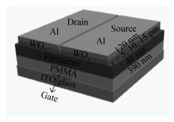
Fig. 1.
The schematic diagram of pentacene-based OFETs with a WO3 buffer layer
SEMICONDUCTOR DEVICES
Jianfeng Fan1, Xiaoman Cheng1, 2, , Xiao Bai1, Lingcheng Zheng1, Jing Jiang1 and Feng Wu1
Corresponding author: Cheng Xiaoman, Email:chengxm@tjut.edu.cn
Abstract: The pentacene-based organic field effect transistor (OFET) with a thin transition metal oxide (WO3) layer between pentacene and metal (Al) source/drain electrodes was fabricated. Compared with conventional OFET with only metal Al source/drain electrodes, the introduction of the WO3 buffer layer leads to the device performance enhancement. The effective field-effect mobility and threshold voltage are improved to 1.90 cm2/(V·s) and 13 V, respectively. The performance improvements are attributed to the decrease of the interface energy barrier and the contact resistance. The results indicate that it is an effective approach to improve the OFET performance by using a WO3 buffer layer.
Keywords: organic field effect transistors, contact resistance, WO3 buffer layer
| [1] |
Zhou L, Wanga A, Wu S C, et al. All-organic active matrix flexible display. Appl Phys Lett, 2006, 88(8):083502 doi: 10.1063/1.2178213
|
| [2] |
Taishi T, Zulkarnaen B, Tetsuo T, et al. High current density in light-emitting transistors of organic single crystals. Phys Rev Lett, 2008, 100(6):066601 doi: 10.1103/PhysRevLett.100.066601
|
| [3] |
Sohn C W, Rim T U, Choi G B, et al. Analysis of contact effects in inverted-staggered organic thin-film transistors based on anisotropic conduction. IEEE Trans Electron Devices, 2010, 57(5):986 doi: 10.1109/TED.2010.2044272
|
| [4] |
Zhao G, Cheng X M, Tian H J, et al. Improved performance of pentacene organic field-effect transistors by inserting a V2O5 metal oxide layer. Chin Phys Lett, 2011, 28(12):127203 doi: 10.1088/0256-307X/28/12/127203
|
| [5] |
Necliudov P V N, Shur M S, Gundlach D J, et al. Contact resistance extraction in pentacene thin film transistors. Solid-State Electron, 2003, 47(2):259 doi: 10.1016/S0038-1101(02)00204-6
|
| [6] |
Kymissis I, Dimitrakopoulos C D, Purushothaman S. High-performance bottom electrode organic thin-film transistors. IEEE Trans Electron Devices, 2001, 48(6):1060 doi: 10.1109/16.925226
|
| [7] |
Bock C, Pham D V, Kunze U, et al. Improved morphology and charge carrier injection in pentacene filed-effect transistors with thiol-treated electrodes. J Appl Phys, 2006, 100(11):114517 doi: 10.1063/1.2400507
|
| [8] |
Chih W C, Li S H, Chen C W, et al. High-performance organic thin-film transistors with metal oxide/metal bilayer electrode. Appl Phys Lett, 2005, 87(19):193508 doi: 10.1063/1.2126140
|
| [9] |
Takatsuka1 Y, Kitamura1 S, Akazawa1 T, et al. Preparation and evaluation of phthalocyanine/vanadium oxide field-effect transistors. International Symposium on Electrical Insulating Materials, 2008:215
|
| [10] |
Darmawan P, Minari T, Kumatani A, et al. Reduction of charge injection barrier by 1-nm contact oxide interlayerin organic field effect transistors. Appl Phys Lett, 2012, 100(1):013303 doi: 10.1063/1.3673842
|
| [11] |
Kröger M, Hamwi S, Meyer J, et al. P-type doping of organic wide band gap materials by transition metal oxides:a case-study on molybdenum trioxide. Org Electron, 2009, 10(5):932 doi: 10.1016/j.orgel.2009.05.007
|
| [12] |
Zhang H M, Choy W C H, Dai Y F, et al. The structural composite effect of Au-WO3-Al interconnecting electrode on performance of each unit in stacked OLEDs. Org Electron, 2009, 10(3):402 doi: 10.1016/j.orgel.2009.01.001
|
| [13] |
Liu Z H, Kobayashi M, Paul B C, et al. Contact engineering for organic semiconductor devices via Fermi level depinning at the metal-organic interface. Phys Rev B, 2010, 82(3):035311 doi: 10.1103/PhysRevB.82.035311
|
| [14] |
Li J, Zhang X W, Zhang L, et al. Improved chromaticity and electron injection in a blue organic light-emitting device by using a dual electron-transport layer with hole-blocking function. Semicond Sci Technol, 2009, 24(7):115012
|
| [15] |
Wang S D, Miyadera T, Minari T, et al. Contact resistance instability in pentacene thin film transistors induced by ambient gases. Appl Phys Lett, 2008, 93(8):043311
|
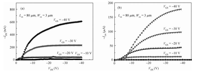
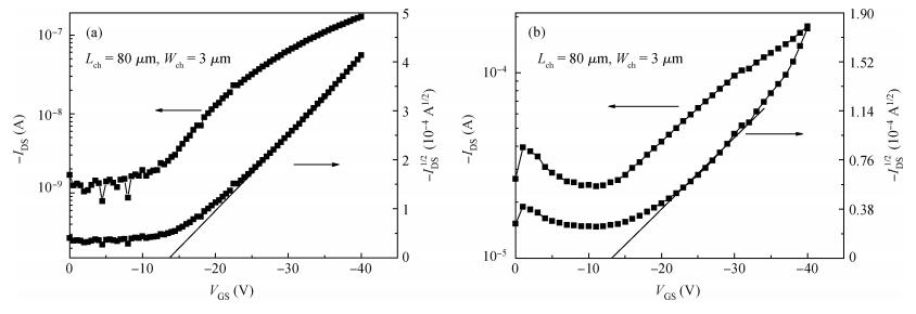
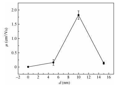
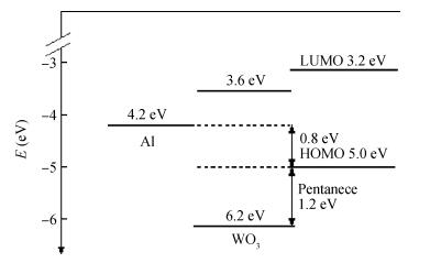
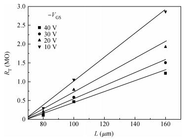
Table 1.
Contact resistances of the OFET with the 10 nm WO3 layer modification at different values of

|
| [1] |
Zhou L, Wanga A, Wu S C, et al. All-organic active matrix flexible display. Appl Phys Lett, 2006, 88(8):083502 doi: 10.1063/1.2178213
|
| [2] |
Taishi T, Zulkarnaen B, Tetsuo T, et al. High current density in light-emitting transistors of organic single crystals. Phys Rev Lett, 2008, 100(6):066601 doi: 10.1103/PhysRevLett.100.066601
|
| [3] |
Sohn C W, Rim T U, Choi G B, et al. Analysis of contact effects in inverted-staggered organic thin-film transistors based on anisotropic conduction. IEEE Trans Electron Devices, 2010, 57(5):986 doi: 10.1109/TED.2010.2044272
|
| [4] |
Zhao G, Cheng X M, Tian H J, et al. Improved performance of pentacene organic field-effect transistors by inserting a V2O5 metal oxide layer. Chin Phys Lett, 2011, 28(12):127203 doi: 10.1088/0256-307X/28/12/127203
|
| [5] |
Necliudov P V N, Shur M S, Gundlach D J, et al. Contact resistance extraction in pentacene thin film transistors. Solid-State Electron, 2003, 47(2):259 doi: 10.1016/S0038-1101(02)00204-6
|
| [6] |
Kymissis I, Dimitrakopoulos C D, Purushothaman S. High-performance bottom electrode organic thin-film transistors. IEEE Trans Electron Devices, 2001, 48(6):1060 doi: 10.1109/16.925226
|
| [7] |
Bock C, Pham D V, Kunze U, et al. Improved morphology and charge carrier injection in pentacene filed-effect transistors with thiol-treated electrodes. J Appl Phys, 2006, 100(11):114517 doi: 10.1063/1.2400507
|
| [8] |
Chih W C, Li S H, Chen C W, et al. High-performance organic thin-film transistors with metal oxide/metal bilayer electrode. Appl Phys Lett, 2005, 87(19):193508 doi: 10.1063/1.2126140
|
| [9] |
Takatsuka1 Y, Kitamura1 S, Akazawa1 T, et al. Preparation and evaluation of phthalocyanine/vanadium oxide field-effect transistors. International Symposium on Electrical Insulating Materials, 2008:215
|
| [10] |
Darmawan P, Minari T, Kumatani A, et al. Reduction of charge injection barrier by 1-nm contact oxide interlayerin organic field effect transistors. Appl Phys Lett, 2012, 100(1):013303 doi: 10.1063/1.3673842
|
| [11] |
Kröger M, Hamwi S, Meyer J, et al. P-type doping of organic wide band gap materials by transition metal oxides:a case-study on molybdenum trioxide. Org Electron, 2009, 10(5):932 doi: 10.1016/j.orgel.2009.05.007
|
| [12] |
Zhang H M, Choy W C H, Dai Y F, et al. The structural composite effect of Au-WO3-Al interconnecting electrode on performance of each unit in stacked OLEDs. Org Electron, 2009, 10(3):402 doi: 10.1016/j.orgel.2009.01.001
|
| [13] |
Liu Z H, Kobayashi M, Paul B C, et al. Contact engineering for organic semiconductor devices via Fermi level depinning at the metal-organic interface. Phys Rev B, 2010, 82(3):035311 doi: 10.1103/PhysRevB.82.035311
|
| [14] |
Li J, Zhang X W, Zhang L, et al. Improved chromaticity and electron injection in a blue organic light-emitting device by using a dual electron-transport layer with hole-blocking function. Semicond Sci Technol, 2009, 24(7):115012
|
| [15] |
Wang S D, Miyadera T, Minari T, et al. Contact resistance instability in pentacene thin film transistors induced by ambient gases. Appl Phys Lett, 2008, 93(8):043311
|


Article views: 2999 Times PDF downloads: 18 Times Cited by: 0 Times
Received: 04 November 2013 Revised: 31 December 2013 Online: Published: 01 June 2014
| Citation: |
Jianfeng Fan, Xiaoman Cheng, Xiao Bai, Lingcheng Zheng, Jing Jiang, Feng Wu. Performance enhancement of pentacene-based organic field-effect transistor by inserting a WO3 buffer layer[J]. Journal of Semiconductors, 2014, 35(6): 064004. doi: 10.1088/1674-4926/35/6/064004
****
J F Fan, X M Cheng, X Bai, L C Zheng, J Jiang, F Wu. Performance enhancement of pentacene-based organic field-effect transistor by inserting a WO3 buffer layer[J]. J. Semicond., 2014, 35(6): 064004. doi: 10.1088/1674-4926/35/6/064004.

|
| [1] |
Zhou L, Wanga A, Wu S C, et al. All-organic active matrix flexible display. Appl Phys Lett, 2006, 88(8):083502 doi: 10.1063/1.2178213
|
| [2] |
Taishi T, Zulkarnaen B, Tetsuo T, et al. High current density in light-emitting transistors of organic single crystals. Phys Rev Lett, 2008, 100(6):066601 doi: 10.1103/PhysRevLett.100.066601
|
| [3] |
Sohn C W, Rim T U, Choi G B, et al. Analysis of contact effects in inverted-staggered organic thin-film transistors based on anisotropic conduction. IEEE Trans Electron Devices, 2010, 57(5):986 doi: 10.1109/TED.2010.2044272
|
| [4] |
Zhao G, Cheng X M, Tian H J, et al. Improved performance of pentacene organic field-effect transistors by inserting a V2O5 metal oxide layer. Chin Phys Lett, 2011, 28(12):127203 doi: 10.1088/0256-307X/28/12/127203
|
| [5] |
Necliudov P V N, Shur M S, Gundlach D J, et al. Contact resistance extraction in pentacene thin film transistors. Solid-State Electron, 2003, 47(2):259 doi: 10.1016/S0038-1101(02)00204-6
|
| [6] |
Kymissis I, Dimitrakopoulos C D, Purushothaman S. High-performance bottom electrode organic thin-film transistors. IEEE Trans Electron Devices, 2001, 48(6):1060 doi: 10.1109/16.925226
|
| [7] |
Bock C, Pham D V, Kunze U, et al. Improved morphology and charge carrier injection in pentacene filed-effect transistors with thiol-treated electrodes. J Appl Phys, 2006, 100(11):114517 doi: 10.1063/1.2400507
|
| [8] |
Chih W C, Li S H, Chen C W, et al. High-performance organic thin-film transistors with metal oxide/metal bilayer electrode. Appl Phys Lett, 2005, 87(19):193508 doi: 10.1063/1.2126140
|
| [9] |
Takatsuka1 Y, Kitamura1 S, Akazawa1 T, et al. Preparation and evaluation of phthalocyanine/vanadium oxide field-effect transistors. International Symposium on Electrical Insulating Materials, 2008:215
|
| [10] |
Darmawan P, Minari T, Kumatani A, et al. Reduction of charge injection barrier by 1-nm contact oxide interlayerin organic field effect transistors. Appl Phys Lett, 2012, 100(1):013303 doi: 10.1063/1.3673842
|
| [11] |
Kröger M, Hamwi S, Meyer J, et al. P-type doping of organic wide band gap materials by transition metal oxides:a case-study on molybdenum trioxide. Org Electron, 2009, 10(5):932 doi: 10.1016/j.orgel.2009.05.007
|
| [12] |
Zhang H M, Choy W C H, Dai Y F, et al. The structural composite effect of Au-WO3-Al interconnecting electrode on performance of each unit in stacked OLEDs. Org Electron, 2009, 10(3):402 doi: 10.1016/j.orgel.2009.01.001
|
| [13] |
Liu Z H, Kobayashi M, Paul B C, et al. Contact engineering for organic semiconductor devices via Fermi level depinning at the metal-organic interface. Phys Rev B, 2010, 82(3):035311 doi: 10.1103/PhysRevB.82.035311
|
| [14] |
Li J, Zhang X W, Zhang L, et al. Improved chromaticity and electron injection in a blue organic light-emitting device by using a dual electron-transport layer with hole-blocking function. Semicond Sci Technol, 2009, 24(7):115012
|
| [15] |
Wang S D, Miyadera T, Minari T, et al. Contact resistance instability in pentacene thin film transistors induced by ambient gases. Appl Phys Lett, 2008, 93(8):043311
|

 WeChat ID
Journal of Semiconductors © 2017 All Rights Reserved 京ICP备05085259号-2

 DownLoad:

