


Fig. 1.
Sketch of 2D graphene lattice with armchair edges. A rectangular elementary cell consisting of 4 carbon atoms, labeled l, $\lambda $ , $\rho$ , r
SEMICONDUCTOR DEVICES
Wei Wang, Gongshu Yue, Xiao Yang, Lu Zhang and Ting Zhang
Corresponding author: Wang Wei, Email:wangwej@njupt.edu.cn
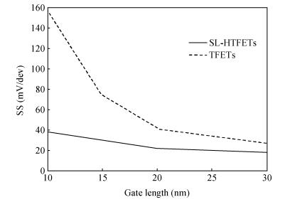
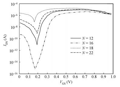
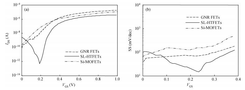
Abstract: We perform a theoretical study of the effects of the lightly doped drain (LDD) and high-k dielectric on the performances of double gate p-i-n tunneling graphene nanoribbon field effect transistors (TFETs). The models are based on non-equilibrium Green's functions (NEGF) solved self-consistently with 3D-Poisson's equations. For the first time, hetero gate dielectric and single LDD TFETs (SL-HTFETs) are proposed and investigated. Simulation results show SL-HTFETs can effectively decrease leakage current, sub-threshold swing, and increase on-off current ratio compared to conventional TFETs and Si-based devices; the SL-HTFETs from the 3p + 1 family have better switching characteristics than those from the 3p family due to smaller effective masses of the former. In addition, comparison of scaled performances between SL-HTFETs and conventional TFETs show that SL-HTFETs have better scaling properties than the conventional TFETs, and thus could be promising devices for logic and ultra-low power applications.
Keywords: GNRFETs, non-equilibrium Green's functions (NEGF), p-i-n tunneling field-effect transistor (TFET), GNR width, lightly doped drain, hetero gate dielectric
| [1] |
Novoselov K S, Geim A K, Morozov S V, et al. Electric field effect in atomically thin carbon films. Science, 2004, 306(5696):666 doi: 10.1126/science.1102896
|
| [2] |
Li X L, Wang X R, Zhang L, et al. Chemically derived, ultrasmooth graphene nanoribbon semiconductors. Science, 2008, 319(5867):1229 doi: 10.1126/science.1150878
|
| [3] |
Geim A K. Graphene:status and prospects. Science, 2009, 324(5934):1530 doi: 10.1126/science.1158877
|
| [4] |
Castro N A H, Guinea F, Peres N M R, et al. The electronic properties of graphene. Rev Mod Phys, 2009, 81(1):109 doi: 10.1103/RevModPhys.81.109
|
| [5] |
Obradovic B, Kotlyar R, Heinz F, et al. Analysis of graphene nanoribbons as a channel material for field-effect transistors. Appl Phys Lett, 2006, 88(14):142102 doi: 10.1063/1.2191420
|
| [6] |
Chen Z, Lin Y M, Rooks M J, et al. Graphene nanoribbon electronics. Phys E, 2007, 40(2):228 doi: 10.1016/j.physe.2007.06.020
|
| [7] |
Brey L, Fertig H A. Electronic states of graphene nanoribbons studied with the Dirac equation. Phys Rev B, 2006, 73(23):235411 doi: 10.1103/PhysRevB.73.235411
|
| [8] |
Zhang Y, Tan Y W, Stormer H L, et al. Experimental observation of the quantum Hall effect and Berry's phase in graphene. Nature, 2005, 438(7065):201 doi: 10.1038/nature04235
|
| [9] |
Lemme M C, Echtermeyer T J, Baus M, et al. A graphene field-effect device. IEEE Electron Device Lett, 2007, 28(4):282 doi: 10.1109/LED.2007.891668
|
| [10] |
Liang G C, Neophytou N, Lundstrom M S, et al. Ballistic graphene nanoribbon metal-oxide-semiconductor field-effect transistors:a full real-space quantum transport simulation. J Appl Phys, 2007, 102(5):054307 doi: 10.1063/1.2775917
|
| [11] |
Lin Y M, Dimitrakopoulos C, Jenkins K A, et al. 100-GHz transistors from wafer-scale epitaxial graphene. Science, 2010, 327(5966):662 doi: 10.1126/science.1184289
|
| [12] |
Liao L, Bai J, Cheng R L, et al. Sub-100 nm channel length graphene transistors. Nano Lett, 2010, 10(10):3952 doi: 10.1021/nl101724k
|
| [13] |
Wu Y, Lin Y, Jenkins K, et al. RF performance of short channel graphene field-effect transistor. Tech Dig Int Electron Device Meeting (IEDM), 2010, 10(6):226
|
| [14] |
Liao L, Lin Y C, Bao M Q, et al. High-speed graphene transistors with a self-aligned nanowire gate. Nature, 2010, 467(7313):305 doi: 10.1038/nature09405
|
| [15] |
Koswatta S O, Lundstrom M S, Nikonov D E. Performance comparison between p-i-n tunneling transistors and conventional MOSFETs. IEEE Trans Electron Devices, 2009, 56(3):456 doi: 10.1109/TED.2008.2011934
|
| [16] |
Klymenko Y, Shevtsov O. Analytical tight-binding approach for ballistic transport through armchair graphene ribbons:exact solutions for propagation through step-like and barrier-like potentials. Phys Rev B, 2008, 77(9):175419
|
| [17] |
Mintmire J W, White C T. Universal density of states for carbon nanotubes. Phys Rev Lett, 1998, 81(12):2506 doi: 10.1103/PhysRevLett.81.2506
|
| [18] |
Fiori G, Iannaccone G. Simulation of graphene nanoribbon field-effect transistors. IEEE Electron Device Lett, 2007, 28(8):760 doi: 10.1109/LED.2007.901680
|
| [19] |
Venugopal R, Paulsson M, Goasguen S, et al. A simple quantum mechanical treatment of scattering nanoscale transistors. J Appl Phys, 2003, 93(9):5613 doi: 10.1063/1.1563298
|
| [20] |
Yeap G C F, Krishnan S, Lin M R. Fringing-induced barrier lowering (FIBL) in sub-100 nm MOSFETs with high-k gate dielectrics. Electron Lett, 1998, 34(11):1150 doi: 10.1049/el:19980800
|
| [21] |
Schlosser M, Bhuwalka K K, Sauter M, et al. Fringing-induced drain current improvement in the tunnel field effect transistor with high-k gate dielectrics. IEEE Trans Electron Devices, 2009, 56(1):100 doi: 10.1109/TED.2008.2008375
|
| [22] |
Kane E O. Zener tunneling in semiconductors. J Phys Chem Solids, 1960, 12(2):181 doi: 10.1016/0022-3697(60)90035-4
|
| [23] |
Chattopadhyay A, Mallik A. Impact of a spacer dielectric and a gate overlap/underlap on the device performance of a tunnel field-effect transistor. IEEE Trans Electron Devices, 2011, 58(3):677 doi: 10.1109/TED.2010.2101603
|
| [24] |
Kliross G S. Gate capacitance modeling and width-dependent performance of grapheme nanoribbon transistors. Microelectron Eng, 2013, 112:220 doi: 10.1016/j.mee.2013.04.011
|
| [25] |
Chin S K, Seah D, Lam K T, et al. Device physics and characteristics of graphene nanoribbon tunneling FETs. IEEE Trans Electron Devices, 2010, 57(11):3144 doi: 10.1109/TED.2010.2065809
|
| [26] |
Choi W Y, Park B G, Lee J D, et al. Tunneling field-effect transistors (TFETs) with sub-threshold swing (SS) less than 60 mV/dec. IEEE Electron Device Lett, 2007, 28(8):743 doi: 10.1109/LED.2007.901273
|


Article views: 2790 Times PDF downloads: 15 Times Cited by: 0 Times
Received: 20 November 2013 Revised: 24 January 2014 Online: Published: 01 June 2014
| Citation: |
Wei Wang, Gongshu Yue, Xiao Yang, Lu Zhang, Ting Zhang. Quantum simulation study of double gate hetero gate dielectric and LDD doping graphene nanoribbon p-i-n tunneling FETs[J]. Journal of Semiconductors, 2014, 35(6): 064006. doi: 10.1088/1674-4926/35/6/064006
****
W Wang, G S Yue, X Yang, L Zhang, T Zhang. Quantum simulation study of double gate hetero gate dielectric and LDD doping graphene nanoribbon p-i-n tunneling FETs[J]. J. Semicond., 2014, 35(6): 064006. doi: 10.1088/1674-4926/35/6/064006.

|
| [1] |
Novoselov K S, Geim A K, Morozov S V, et al. Electric field effect in atomically thin carbon films. Science, 2004, 306(5696):666 doi: 10.1126/science.1102896
|
| [2] |
Li X L, Wang X R, Zhang L, et al. Chemically derived, ultrasmooth graphene nanoribbon semiconductors. Science, 2008, 319(5867):1229 doi: 10.1126/science.1150878
|
| [3] |
Geim A K. Graphene:status and prospects. Science, 2009, 324(5934):1530 doi: 10.1126/science.1158877
|
| [4] |
Castro N A H, Guinea F, Peres N M R, et al. The electronic properties of graphene. Rev Mod Phys, 2009, 81(1):109 doi: 10.1103/RevModPhys.81.109
|
| [5] |
Obradovic B, Kotlyar R, Heinz F, et al. Analysis of graphene nanoribbons as a channel material for field-effect transistors. Appl Phys Lett, 2006, 88(14):142102 doi: 10.1063/1.2191420
|
| [6] |
Chen Z, Lin Y M, Rooks M J, et al. Graphene nanoribbon electronics. Phys E, 2007, 40(2):228 doi: 10.1016/j.physe.2007.06.020
|
| [7] |
Brey L, Fertig H A. Electronic states of graphene nanoribbons studied with the Dirac equation. Phys Rev B, 2006, 73(23):235411 doi: 10.1103/PhysRevB.73.235411
|
| [8] |
Zhang Y, Tan Y W, Stormer H L, et al. Experimental observation of the quantum Hall effect and Berry's phase in graphene. Nature, 2005, 438(7065):201 doi: 10.1038/nature04235
|
| [9] |
Lemme M C, Echtermeyer T J, Baus M, et al. A graphene field-effect device. IEEE Electron Device Lett, 2007, 28(4):282 doi: 10.1109/LED.2007.891668
|
| [10] |
Liang G C, Neophytou N, Lundstrom M S, et al. Ballistic graphene nanoribbon metal-oxide-semiconductor field-effect transistors:a full real-space quantum transport simulation. J Appl Phys, 2007, 102(5):054307 doi: 10.1063/1.2775917
|
| [11] |
Lin Y M, Dimitrakopoulos C, Jenkins K A, et al. 100-GHz transistors from wafer-scale epitaxial graphene. Science, 2010, 327(5966):662 doi: 10.1126/science.1184289
|
| [12] |
Liao L, Bai J, Cheng R L, et al. Sub-100 nm channel length graphene transistors. Nano Lett, 2010, 10(10):3952 doi: 10.1021/nl101724k
|
| [13] |
Wu Y, Lin Y, Jenkins K, et al. RF performance of short channel graphene field-effect transistor. Tech Dig Int Electron Device Meeting (IEDM), 2010, 10(6):226
|
| [14] |
Liao L, Lin Y C, Bao M Q, et al. High-speed graphene transistors with a self-aligned nanowire gate. Nature, 2010, 467(7313):305 doi: 10.1038/nature09405
|
| [15] |
Koswatta S O, Lundstrom M S, Nikonov D E. Performance comparison between p-i-n tunneling transistors and conventional MOSFETs. IEEE Trans Electron Devices, 2009, 56(3):456 doi: 10.1109/TED.2008.2011934
|
| [16] |
Klymenko Y, Shevtsov O. Analytical tight-binding approach for ballistic transport through armchair graphene ribbons:exact solutions for propagation through step-like and barrier-like potentials. Phys Rev B, 2008, 77(9):175419
|
| [17] |
Mintmire J W, White C T. Universal density of states for carbon nanotubes. Phys Rev Lett, 1998, 81(12):2506 doi: 10.1103/PhysRevLett.81.2506
|
| [18] |
Fiori G, Iannaccone G. Simulation of graphene nanoribbon field-effect transistors. IEEE Electron Device Lett, 2007, 28(8):760 doi: 10.1109/LED.2007.901680
|
| [19] |
Venugopal R, Paulsson M, Goasguen S, et al. A simple quantum mechanical treatment of scattering nanoscale transistors. J Appl Phys, 2003, 93(9):5613 doi: 10.1063/1.1563298
|
| [20] |
Yeap G C F, Krishnan S, Lin M R. Fringing-induced barrier lowering (FIBL) in sub-100 nm MOSFETs with high-k gate dielectrics. Electron Lett, 1998, 34(11):1150 doi: 10.1049/el:19980800
|
| [21] |
Schlosser M, Bhuwalka K K, Sauter M, et al. Fringing-induced drain current improvement in the tunnel field effect transistor with high-k gate dielectrics. IEEE Trans Electron Devices, 2009, 56(1):100 doi: 10.1109/TED.2008.2008375
|
| [22] |
Kane E O. Zener tunneling in semiconductors. J Phys Chem Solids, 1960, 12(2):181 doi: 10.1016/0022-3697(60)90035-4
|
| [23] |
Chattopadhyay A, Mallik A. Impact of a spacer dielectric and a gate overlap/underlap on the device performance of a tunnel field-effect transistor. IEEE Trans Electron Devices, 2011, 58(3):677 doi: 10.1109/TED.2010.2101603
|
| [24] |
Kliross G S. Gate capacitance modeling and width-dependent performance of grapheme nanoribbon transistors. Microelectron Eng, 2013, 112:220 doi: 10.1016/j.mee.2013.04.011
|
| [25] |
Chin S K, Seah D, Lam K T, et al. Device physics and characteristics of graphene nanoribbon tunneling FETs. IEEE Trans Electron Devices, 2010, 57(11):3144 doi: 10.1109/TED.2010.2065809
|
| [26] |
Choi W Y, Park B G, Lee J D, et al. Tunneling field-effect transistors (TFETs) with sub-threshold swing (SS) less than 60 mV/dec. IEEE Electron Device Lett, 2007, 28(8):743 doi: 10.1109/LED.2007.901273
|

 WeChat ID
Journal of Semiconductors © 2017 All Rights Reserved 京ICP备05085259号-2

 DownLoad:

