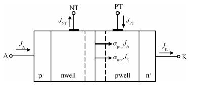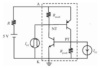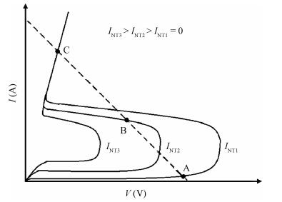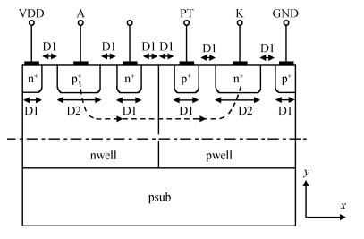
Fig. 1.
Schematic Cross section of DTSCR structure.
SEMICONDUCTOR DEVICES
Jizhi Liu1, , Zhiwei Liu1, Ze Jia1 and Juin. J Liou2
Corresponding author: Liu Jizhi, Email:jzhliu@uestc.edu.cn
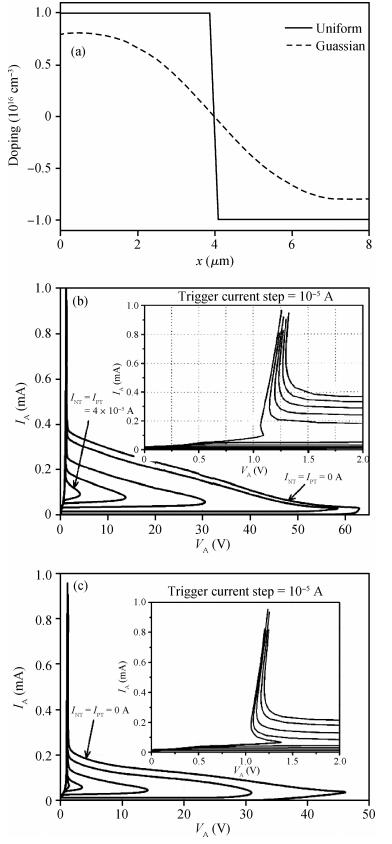
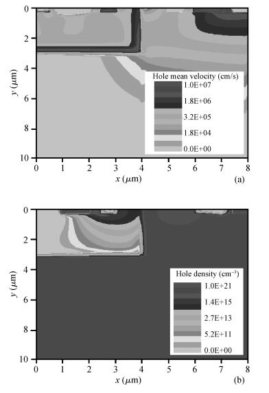
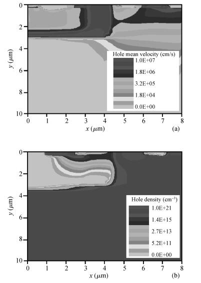
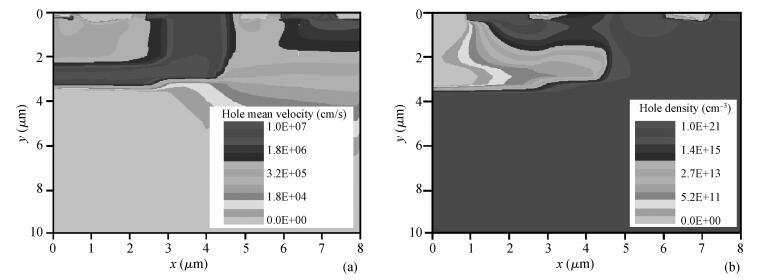
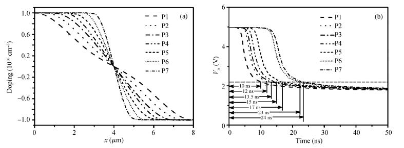
Abstract: The turn-on speed of electrostatic discharge (ESD) protection devices is very important for the protection of the ultrathin gate oxide. A double trigger silicon controlled rectifier device (DTSCR) can be used effectively for ESD protection because it can turn on relatively quickly. The turn-on process of the DTSCR is first studied, and a formula for calculating the turn-on time of the DTSCR is derived. It is found that the turn-on time of the DTSCR is determined mainly by the base transit time of the parasitic p-n-p and n-p-n transistors. Using the variation lateral base doping (VLBD) structure can reduce the base transit time, and a novel DTSCR device with a VLBD structure (VLBD_DTSCR) is proposed for ESD protection applications. The static-state and turn-on characteristics of the VLBD_DTSCR device are simulated. The simulation results show that the VLBD structure can introduce a built-in electric field in the base region of the parasitic n-p-n and p-n-p bipolar transistors to accelerate the transport of free-carriers through the base region. In the same process and layout area, the turn-on time of the VLBD_DTSCR device is at least 27% less than that of the DTSCR device with the traditional uniform base doping under the same value of the trigger current.
Keywords: electrostatic discharge (ESD), double triggered silicon controlled rectifier (DTSCR), variation lateral base doping (VLBD), built-in electric field, turn-on speed
| [1] |
Ker M D, Hsu K C. Overview of on-chip electrostatic discharge protection design with SCR-based devices in CMOS integrated circuits. IEEE Trans Device Mater Rel, 2005, 5(2):235 doi: 10.1109/TDMR.2005.846824
|
| [2] |
Wu J, Juliano P, Rosenbaum E. Breakdown and latent damage of ultra-thin gate oxides under ESD stress conditions. Proc EOS/ESD Symp, Anaheim, CA, 2000:287 http://www.doc88.com/p-598167111306.html
|
| [3] |
ESD Association. ESD Association Standard Test Method for Electrostatic Discharge Sensitivity Testing: Charged Device Model-Component Level, ESD STM 5. 3. 1, 1999
|
| [4] |
Ker M D, Hsu K C. Substrate-triggered SCR device for on-chip ESD protection in fully silicided sub-0.25-μm CMOS process. IEEE Trans Electron Devices, 2003, 50(2):397 doi: 10.1109/TED.2003.809028
|
| [5] |
Mergens M P J, Russ C C, Verhaege K G, et al. Speed optimized diode-triggered SCR (DTSCR) for RF ESD protection of ultra-sensitive IC nodes in advanced technologies. IEEE Trans Device Mater Reliab, 2005, 5(3):532 doi: 10.1109/TDMR.2005.853510
|
| [6] |
Russ C, Mergens M P J, Armer J, et al. GGSCR:GGNMOS triggered silicon controlled rectifiers for ESD protection in deep submicron CMOS processes. Proc EOS/ESD Symp, 2001:22 http://ieeexplore.ieee.org/xpls/icp.jsp?arnumber=5254990
|
| [7] |
Mergens M P J, Russ C C, Verhage K G, et al. High holding current SCRs (HHI-SCR) for ESD protection and latch-up immune IC operation. Proc EOS/ESD Symp, 2002:10 https://core.ac.uk/display/24706588
|
| [8] |
Ker M D, Hsu K C. Latchup-free ESD protection design with complementary substrate-triggered SCR devices. IEEE J Solid-State Circuits, 2003, 38(8):1380 doi: 10.1109/JSSC.2003.814434
|
| [9] |
Lin C Y, Chu L W, Ker M D, et al. ESD protection structure with inductor-triggered SCR for RF applications in 65-nm CMOS process. Proc IRPS Symp, 2012:EL.3.1 http://ieeexplore.ieee.org/document/6241893/authors
|
| [10] |
Ker M D, Hsu K C. SCR devices with double-triggered technique for on-chip ESD protection in sub-quarter-micron silicided CMOS processes. IEEE Trans Device Mater Reliab, 2003, 3(3):58 doi: 10.1109/TDMR.2003.815192
|
| [11] |
Kuhn W, Kuhn W, Eatinger R, et al. ESD detection circuit and associated metal fuse investigations in CMOS processes. IEEE Trans Device Mater Reliab, 2014, PP(1):1 http://ieeexplore.ieee.org/xpl/articleDetails.jsp?arnumber=6697836&punumber%3D7298
|
| [12] |
Liu H, Yang Z, Zhuo Q. Two ESD detection circuits for 3x VDD-tolerant I/O buffer in low-voltage CMOS processes with low leakage currents. IEEE Trans Device Mater Reliab, 2013, 13(1):319 doi: 10.1109/TDMR.2012.2218606
|
| [13] |
Altolaguirre F A, Ker M D. Power-rail ESD clamp circuit with diode-string ESD detection to overcome the gate leakage current in a 40-nm CMOS process. IEEE Trans Electron Devices, 2013, 60(10):3500 doi: 10.1109/TED.2013.2274701
|
| [14] |
Yeh C T, Ker M D. High area-efficient ESD clamp circuit with equivalent RC-based detection mechanism in a 65-nm CMOS process. IEEE Trans Electron Devices, 2013, 60(3):1011 doi: 10.1109/TED.2013.2241441
|
| [15] |
Yeh C T, Ker M D. ESD-transient detection circuit with equivalent capacitance-coupling detection mechanism and high efficiency of layout area in a 65nm CMOS technology. Electrical Overstress/Electrostatic Discharge Symposium (EOS/ESD), 2013:1 http://ieeexplore.ieee.org/xpl/abstractAuthors.jsp?reload=true&arnumber=6635907&punumber%3D6619544
|
| [16] |
Muller R S, Kamins T I. Device electronics for integrated circuits. 3rd ed. New York:Wiley, 2002:337
|
| [17] |
Chen X B, Zhang Q Z, Chen Y. Microelectric devices. 2nd ed. Beijing:Electronic Industry Press, 2005:91
|
| [18] |
Webster W M. On the variation of junction-transistor current-amplification factor with emitter current. Proc IRE, 1954:914 http://ieeexplore.ieee.org/xpls/abs_all.jsp?isnumber=4051702&arnumber=4051728&count=36&index=23
|
| [19] |
Baliga B J. Fundamentals of power semiconductor devices. New York:Springer, 2008:662
|
| [20] |
Merchant S. Arbitrary lateral diffusion profiles. IEEE Trans Electron Devices, 1995, 42(12):2226 doi: 10.1109/16.477783
|
| [21] |
Stengl R, Gösele U. Variation of lateral doping-a new concept to avoid high-voltage breakdown of planar junctions. IEDM Tech Dig, 1985:154 http://ieeexplore.ieee.org/xpls/abs_all.jsp?arnumber=1485467
|
| [22] |
Zhang S, Sin J K O, Lai T M L, et al. Numerical modeling of linear doping profiles for high-voltage thin-film SOI devices. IEEE Trans Electron Devices, 1999, 46(9):1036 http://ieeexplore.ieee.org/xpl/abstractKeywords.jsp?reload=true&arnumber=760414&pageNumber%3D31914%26rowsPerPage%3D100
|
| [23] |
Hardikar S, Tadikonda R, Green D W, et al. Realizing high-voltage junction isolated LDMOS transistors with variation in lateral doping. IEEE Trans Electron Devices, 2004, 51(12):2223 doi: 10.1109/TED.2004.839104
|
| [24] |
Sarro J D, Chatty K, Gauthier R, et al. Study of design factors affecting turn-on time of silicon controlled rectifiers (SCRs) in 90nm and 60nm bulk CMOS technologies. Proc IRPS Symp, 2006:163 http://ieeexplore.ieee.org/document/4017151/
|


Article views: 3367 Times PDF downloads: 30 Times Cited by: 0 Times
Received: 22 December 2013 Revised: 09 January 2014 Online: Published: 01 June 2014
| Citation: |
Jizhi Liu, Zhiwei Liu, Ze Jia, Juin. J Liou. A novel DTSCR with a variation lateral base doping structure to improve turn-on speed for ESD protection[J]. Journal of Semiconductors, 2014, 35(6): 064010. doi: 10.1088/1674-4926/35/6/064010
****
J Z Liu, Z W Liu, Z Jia, Juin. J J Liou. A novel DTSCR with a variation lateral base doping structure to improve turn-on speed for ESD protection[J]. J. Semicond., 2014, 35(6): 064010. doi: 10.1088/1674-4926/35/6/064010.

|
| [1] |
Ker M D, Hsu K C. Overview of on-chip electrostatic discharge protection design with SCR-based devices in CMOS integrated circuits. IEEE Trans Device Mater Rel, 2005, 5(2):235 doi: 10.1109/TDMR.2005.846824
|
| [2] |
Wu J, Juliano P, Rosenbaum E. Breakdown and latent damage of ultra-thin gate oxides under ESD stress conditions. Proc EOS/ESD Symp, Anaheim, CA, 2000:287 http://www.doc88.com/p-598167111306.html
|
| [3] |
ESD Association. ESD Association Standard Test Method for Electrostatic Discharge Sensitivity Testing: Charged Device Model-Component Level, ESD STM 5. 3. 1, 1999
|
| [4] |
Ker M D, Hsu K C. Substrate-triggered SCR device for on-chip ESD protection in fully silicided sub-0.25-μm CMOS process. IEEE Trans Electron Devices, 2003, 50(2):397 doi: 10.1109/TED.2003.809028
|
| [5] |
Mergens M P J, Russ C C, Verhaege K G, et al. Speed optimized diode-triggered SCR (DTSCR) for RF ESD protection of ultra-sensitive IC nodes in advanced technologies. IEEE Trans Device Mater Reliab, 2005, 5(3):532 doi: 10.1109/TDMR.2005.853510
|
| [6] |
Russ C, Mergens M P J, Armer J, et al. GGSCR:GGNMOS triggered silicon controlled rectifiers for ESD protection in deep submicron CMOS processes. Proc EOS/ESD Symp, 2001:22 http://ieeexplore.ieee.org/xpls/icp.jsp?arnumber=5254990
|
| [7] |
Mergens M P J, Russ C C, Verhage K G, et al. High holding current SCRs (HHI-SCR) for ESD protection and latch-up immune IC operation. Proc EOS/ESD Symp, 2002:10 https://core.ac.uk/display/24706588
|
| [8] |
Ker M D, Hsu K C. Latchup-free ESD protection design with complementary substrate-triggered SCR devices. IEEE J Solid-State Circuits, 2003, 38(8):1380 doi: 10.1109/JSSC.2003.814434
|
| [9] |
Lin C Y, Chu L W, Ker M D, et al. ESD protection structure with inductor-triggered SCR for RF applications in 65-nm CMOS process. Proc IRPS Symp, 2012:EL.3.1 http://ieeexplore.ieee.org/document/6241893/authors
|
| [10] |
Ker M D, Hsu K C. SCR devices with double-triggered technique for on-chip ESD protection in sub-quarter-micron silicided CMOS processes. IEEE Trans Device Mater Reliab, 2003, 3(3):58 doi: 10.1109/TDMR.2003.815192
|
| [11] |
Kuhn W, Kuhn W, Eatinger R, et al. ESD detection circuit and associated metal fuse investigations in CMOS processes. IEEE Trans Device Mater Reliab, 2014, PP(1):1 http://ieeexplore.ieee.org/xpl/articleDetails.jsp?arnumber=6697836&punumber%3D7298
|
| [12] |
Liu H, Yang Z, Zhuo Q. Two ESD detection circuits for 3x VDD-tolerant I/O buffer in low-voltage CMOS processes with low leakage currents. IEEE Trans Device Mater Reliab, 2013, 13(1):319 doi: 10.1109/TDMR.2012.2218606
|
| [13] |
Altolaguirre F A, Ker M D. Power-rail ESD clamp circuit with diode-string ESD detection to overcome the gate leakage current in a 40-nm CMOS process. IEEE Trans Electron Devices, 2013, 60(10):3500 doi: 10.1109/TED.2013.2274701
|
| [14] |
Yeh C T, Ker M D. High area-efficient ESD clamp circuit with equivalent RC-based detection mechanism in a 65-nm CMOS process. IEEE Trans Electron Devices, 2013, 60(3):1011 doi: 10.1109/TED.2013.2241441
|
| [15] |
Yeh C T, Ker M D. ESD-transient detection circuit with equivalent capacitance-coupling detection mechanism and high efficiency of layout area in a 65nm CMOS technology. Electrical Overstress/Electrostatic Discharge Symposium (EOS/ESD), 2013:1 http://ieeexplore.ieee.org/xpl/abstractAuthors.jsp?reload=true&arnumber=6635907&punumber%3D6619544
|
| [16] |
Muller R S, Kamins T I. Device electronics for integrated circuits. 3rd ed. New York:Wiley, 2002:337
|
| [17] |
Chen X B, Zhang Q Z, Chen Y. Microelectric devices. 2nd ed. Beijing:Electronic Industry Press, 2005:91
|
| [18] |
Webster W M. On the variation of junction-transistor current-amplification factor with emitter current. Proc IRE, 1954:914 http://ieeexplore.ieee.org/xpls/abs_all.jsp?isnumber=4051702&arnumber=4051728&count=36&index=23
|
| [19] |
Baliga B J. Fundamentals of power semiconductor devices. New York:Springer, 2008:662
|
| [20] |
Merchant S. Arbitrary lateral diffusion profiles. IEEE Trans Electron Devices, 1995, 42(12):2226 doi: 10.1109/16.477783
|
| [21] |
Stengl R, Gösele U. Variation of lateral doping-a new concept to avoid high-voltage breakdown of planar junctions. IEDM Tech Dig, 1985:154 http://ieeexplore.ieee.org/xpls/abs_all.jsp?arnumber=1485467
|
| [22] |
Zhang S, Sin J K O, Lai T M L, et al. Numerical modeling of linear doping profiles for high-voltage thin-film SOI devices. IEEE Trans Electron Devices, 1999, 46(9):1036 http://ieeexplore.ieee.org/xpl/abstractKeywords.jsp?reload=true&arnumber=760414&pageNumber%3D31914%26rowsPerPage%3D100
|
| [23] |
Hardikar S, Tadikonda R, Green D W, et al. Realizing high-voltage junction isolated LDMOS transistors with variation in lateral doping. IEEE Trans Electron Devices, 2004, 51(12):2223 doi: 10.1109/TED.2004.839104
|
| [24] |
Sarro J D, Chatty K, Gauthier R, et al. Study of design factors affecting turn-on time of silicon controlled rectifiers (SCRs) in 90nm and 60nm bulk CMOS technologies. Proc IRPS Symp, 2006:163 http://ieeexplore.ieee.org/document/4017151/
|

 WeChat ID
Journal of Semiconductors © 2017 All Rights Reserved 京ICP备05085259号-2

 DownLoad: